element14 Community
element14 Community
    Register Log In
  • Site
  • Search
  • Log In Register
  • Community Hub
    Community Hub
    • What's New on element14
    • Feedback and Support
    • Benefits of Membership
    • Personal Blogs
    • Members Area
    • Achievement Levels
  • Learn
    Learn
    • Ask an Expert
    • eBooks
    • element14 presents
    • Learning Center
    • Tech Spotlight
    • STEM Academy
    • Webinars, Training and Events
    • Learning Groups
  • Technologies
    Technologies
    • 3D Printing
    • FPGA
    • Industrial Automation
    • Internet of Things
    • Power & Energy
    • Sensors
    • Technology Groups
  • Challenges & Projects
    Challenges & Projects
    • Design Challenges
    • element14 presents Projects
    • Project14
    • Arduino Projects
    • Raspberry Pi Projects
    • Project Groups
  • Products
    Products
    • Arduino
    • Avnet Boards Community
    • Dev Tools
    • Manufacturers
    • Multicomp Pro
    • Product Groups
    • Raspberry Pi
    • RoadTests & Reviews
  • Store
    Store
    • Visit Your Store
    • Choose another store...
      • Europe
      •  Austria (German)
      •  Belgium (Dutch, French)
      •  Bulgaria (Bulgarian)
      •  Czech Republic (Czech)
      •  Denmark (Danish)
      •  Estonia (Estonian)
      •  Finland (Finnish)
      •  France (French)
      •  Germany (German)
      •  Hungary (Hungarian)
      •  Ireland
      •  Israel
      •  Italy (Italian)
      •  Latvia (Latvian)
      •  
      •  Lithuania (Lithuanian)
      •  Netherlands (Dutch)
      •  Norway (Norwegian)
      •  Poland (Polish)
      •  Portugal (Portuguese)
      •  Romania (Romanian)
      •  Russia (Russian)
      •  Slovakia (Slovak)
      •  Slovenia (Slovenian)
      •  Spain (Spanish)
      •  Sweden (Swedish)
      •  Switzerland(German, French)
      •  Turkey (Turkish)
      •  United Kingdom
      • Asia Pacific
      •  Australia
      •  China
      •  Hong Kong
      •  India
      •  Korea (Korean)
      •  Malaysia
      •  New Zealand
      •  Philippines
      •  Singapore
      •  Taiwan
      •  Thailand (Thai)
      • Americas
      •  Brazil (Portuguese)
      •  Canada
      •  Mexico (Spanish)
      •  United States
      Can't find the country/region you're looking for? Visit our export site or find a local distributor.
  • Translate
  • Profile
  • Settings
Altium CircuitStudio
  • Products
  • Manufacturers
  • Altium CircuitStudio
  • More
  • Cancel
Altium CircuitStudio
Altium CircuitStudio Forum Design Rule Verification
  • Blog
  • Forum
  • Documents
  • Events
  • Polls
  • Members
  • Mentions
  • Sub-Groups
  • Tags
  • More
  • Cancel
  • New
Join Altium CircuitStudio to participate - click to join for free!
Actions
  • Share
  • More
  • Cancel
Forum Thread Details
  • Locked Locked
  • Replies 9 replies
  • Subscribers 87 subscribers
  • Views 703 views
  • Users 0 members are here
Related
This discussion has been locked.
You can no longer post new replies to this discussion. If you have a question you can start a new discussion

Design Rule Verification

dmitriy2020
dmitriy2020 over 5 years ago

Hello.

I make multilayer PCB with blind and buried vias. I have a problem with rule verification.

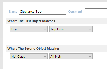
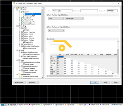
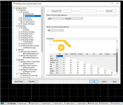
The rules was made for each layers separately . That way is convenient for my design.

for example 0.1mm:

image

image

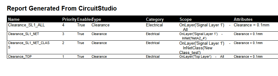
There are blind via (TOP- Signal layer 1) and buried via (Signal layer 1- Signal layer 6 ).  Both of vias are on the Signal layer 1 with distance 0.06mm. 

image

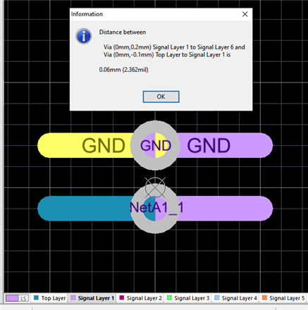
1 Checking design rules does not give any errors though the gap is only 0.06mm on Signal layer 1.

2 If I use a general rule for all leyers  I will get the correct сlearance  constraint error.


Why the rule does not work in the first case? Could you help me with rules for separate layers.

  • Cancel

Top Replies

  • voltsandjolts
    voltsandjolts over 5 years ago in reply to dmitriy2020 +1
    I think there might be a bug. To me, it looks like if you have a clearance rule specifying layer (e.g. Top Layer - ALL) then: Track to track is checked OK Track to via is checked OK Via to Via is NOT checked…
  • voltsandjolts
    voltsandjolts over 5 years ago

    Try this:


    image

    • Cancel
    • Vote Up 0 Vote Down
    • Cancel
  • voltsandjolts
    voltsandjolts over 5 years ago

    You can add net classes to get different clearances as required.

    You can use the net class directive on the schematic or, if you need lots of those, it's easier to use net blankets:

    https://www.eevblog.com/forum/circuit-studio/net-blankets-for-circuitstudio/

    • Cancel
    • Vote Up 0 Vote Down
    • Cancel
  • dmitriy2020
    dmitriy2020 over 5 years ago in reply to voltsandjolts

    This way (OnLayer('Signal Layer 1') -  InNetClass('All Nets')  Clearance = 0.1mm )  doesn't work too. It look like a bug of CircuitStudio . Can you confirm that the case is repeated on your computer?

    • Cancel
    • Vote Up 0 Vote Down
    • Cancel
  • voltsandjolts
    voltsandjolts over 5 years ago in reply to dmitriy2020

    Can you provide a simple CsPcbDoc here that shows the problem, thanks.


    Check online DRC is enabled;

    File > System Preferences > PCB Editor > General > Online DRC

    • Cancel
    • Vote Up 0 Vote Down
    • Cancel
  • dmitriy2020
    dmitriy2020 over 5 years ago in reply to voltsandjolts

    There is online DRC. I tried several variants :

    image

    still not getting any error

    Please check CsPcbDoc :

    Attachments:
    new_pcb_test.zip
    • Cancel
    • Vote Up 0 Vote Down
    • Cancel
  • voltsandjolts
    voltsandjolts over 5 years ago in reply to dmitriy2020

    I think there might be a bug.

    To me, it looks like if you have a clearance rule specifying layer (e.g. Top Layer - ALL) then:

    Track to track is checked OK

    Track to via is checked OK

    Via to Via is NOT checked


    Edit:

    Ah, its not a bug, it needs another rule.

    Vias (and TH-pads) are "Multi-Layer" objects so a rule like [Top Layer - ALL] does not apply to them. They are not on the "Top Layer" ... not intuitive logic I would say, but thats the way it is.


    Create an additional rule for via/pad clearance to other vias/pads.

    (Enter -1 for Minimum Clearance then enter clearance values)


    image

    • Cancel
    • Vote Up +1 Vote Down
    • Cancel
  • dmitriy2020
    dmitriy2020 over 5 years ago in reply to voltsandjolts

    It is worth noting  Your rule is not for signal layer 1. No doubt, general rules are work well.


    I think the bug appears for blind and buried vias on selected layers only. The rule is not checked between rings of vias .

    • Cancel
    • Vote Up 0 Vote Down
    • Cancel
  • voltsandjolts
    voltsandjolts over 5 years ago in reply to dmitriy2020

    Correct, the above rule and clearance apply to all layers.

    So, you would need to use worst case clearance value for all layers.

    I can't see a way to to specify via-to-via clearance differently for each layer.

    Please post here if you find a way.


    Are you saying the rule I posted above is not applied to blind and buried vias?

    • Cancel
    • Vote Up 0 Vote Down
    • Cancel
  • dmitriy2020
    dmitriy2020 over 5 years ago in reply to voltsandjolts

    Thanks for the help. I will follow your recommendations.

    • Cancel
    • Vote Up 0 Vote Down
    • Cancel
element14 Community

element14 is the first online community specifically for engineers. Connect with your peers and get expert answers to your questions.

  • Members
  • Learn
  • Technologies
  • Challenges & Projects
  • Products
  • Store
  • About Us
  • Feedback & Support
  • FAQs
  • Terms of Use
  • Privacy Policy
  • Legal and Copyright Notices
  • Sitemap
  • Cookies

An Avnet Company © 2025 Premier Farnell Limited. All Rights Reserved.

Premier Farnell Ltd, registered in England and Wales (no 00876412), registered office: Farnell House, Forge Lane, Leeds LS12 2NE.

ICP 备案号 10220084.

Follow element14

  • X
  • Facebook
  • linkedin
  • YouTube