element14 Community
element14 Community
    Register Log In
  • Site
  • Search
  • Log In Register
  • About Us
  • Community Hub
    Community Hub
    • What's New on element14
    • Feedback and Support
    • Benefits of Membership
    • Personal Blogs
    • Members Area
    • Achievement Levels
  • Learn
    Learn
    • Ask an Expert
    • eBooks
    • element14 presents
    • Learning Center
    • Tech Spotlight
    • STEM Academy
    • Webinars, Training and Events
    • Learning Groups
  • Technologies
    Technologies
    • 3D Printing
    • FPGA
    • Industrial Automation
    • Internet of Things
    • Power & Energy
    • Sensors
    • Technology Groups
  • Challenges & Projects
    Challenges & Projects
    • Design Challenges
    • element14 presents Projects
    • Project14
    • Arduino Projects
    • Raspberry Pi Projects
    • Project Groups
  • Products
    Products
    • Arduino
    • Avnet Boards Community
    • Dev Tools
    • Manufacturers
    • Multicomp Pro
    • Product Groups
    • Raspberry Pi
    • RoadTests & Reviews
  • Store
    Store
    • Visit Your Store
    • Choose another store...
      • Europe
      •  Austria (German)
      •  Belgium (Dutch, French)
      •  Bulgaria (Bulgarian)
      •  Czech Republic (Czech)
      •  Denmark (Danish)
      •  Estonia (Estonian)
      •  Finland (Finnish)
      •  France (French)
      •  Germany (German)
      •  Hungary (Hungarian)
      •  Ireland
      •  Israel
      •  Italy (Italian)
      •  Latvia (Latvian)
      •  
      •  Lithuania (Lithuanian)
      •  Netherlands (Dutch)
      •  Norway (Norwegian)
      •  Poland (Polish)
      •  Portugal (Portuguese)
      •  Romania (Romanian)
      •  Russia (Russian)
      •  Slovakia (Slovak)
      •  Slovenia (Slovenian)
      •  Spain (Spanish)
      •  Sweden (Swedish)
      •  Switzerland(German, French)
      •  Turkey (Turkish)
      •  United Kingdom
      • Asia Pacific
      •  Australia
      •  China
      •  Hong Kong
      •  India
      •  Korea (Korean)
      •  Malaysia
      •  New Zealand
      •  Philippines
      •  Singapore
      •  Taiwan
      •  Thailand (Thai)
      • Americas
      •  Brazil (Portuguese)
      •  Canada
      •  Mexico (Spanish)
      •  United States
      Can't find the country/region you're looking for? Visit our export site or find a local distributor.
  • Translate
  • Profile
  • Settings
Altium CircuitStudio
  • Products
  • Manufacturers
  • Altium CircuitStudio
  • More
  • Cancel
Altium CircuitStudio
Altium CircuitStudio Forum How to Assign Net Name to Internal Layer
  • Blog
  • Forum
  • Documents
  • Events
  • Polls
  • Members
  • Mentions
  • Sub-Groups
  • Tags
  • More
  • Cancel
  • New
Join Altium CircuitStudio to participate - click to join for free!
Actions
  • Share
  • More
  • Cancel
Forum Thread Details
  • State Not Answered
  • Locked Locked
  • Replies 6 replies
  • Subscribers 88 subscribers
  • Views 1407 views
  • Users 0 members are here
  • internal layers
Related
This discussion has been locked.
You can no longer post new replies to this discussion. If you have a question you can start a new discussion

How to Assign Net Name to Internal Layer

mflux_gamble
mflux_gamble over 8 years ago

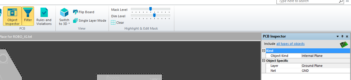
Seems silly, but I do not see a way to assign a net name to an internal layer.


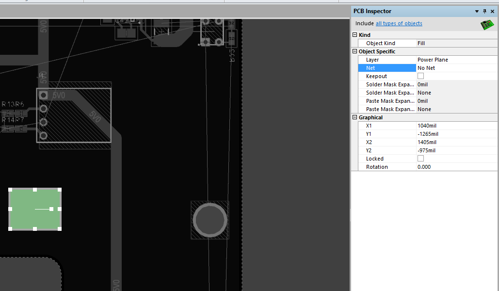
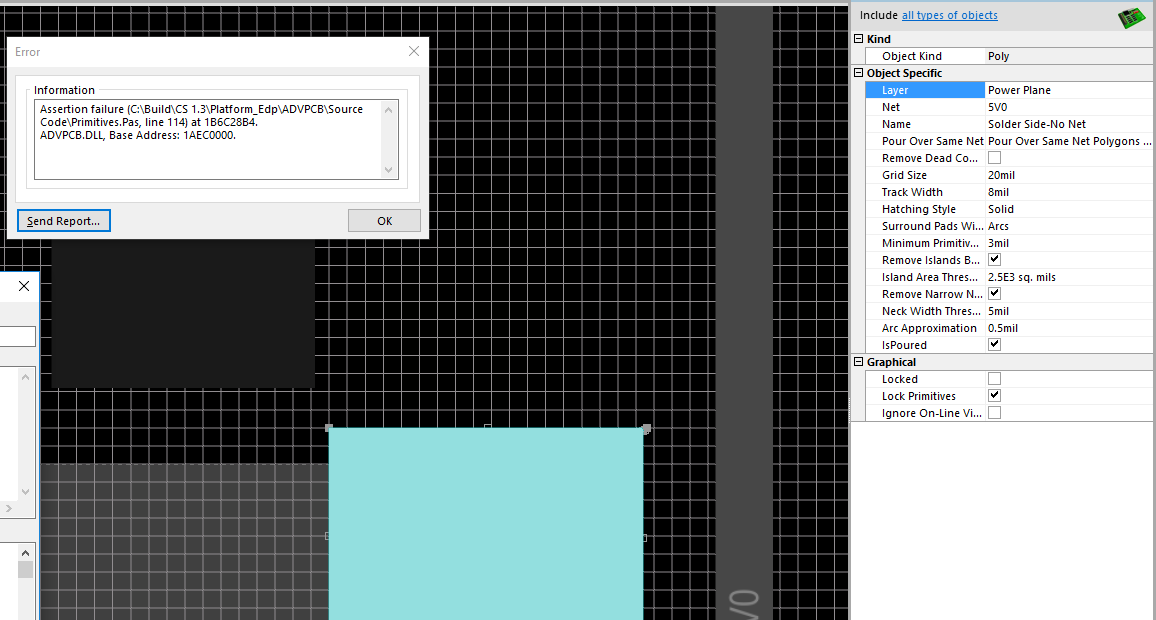
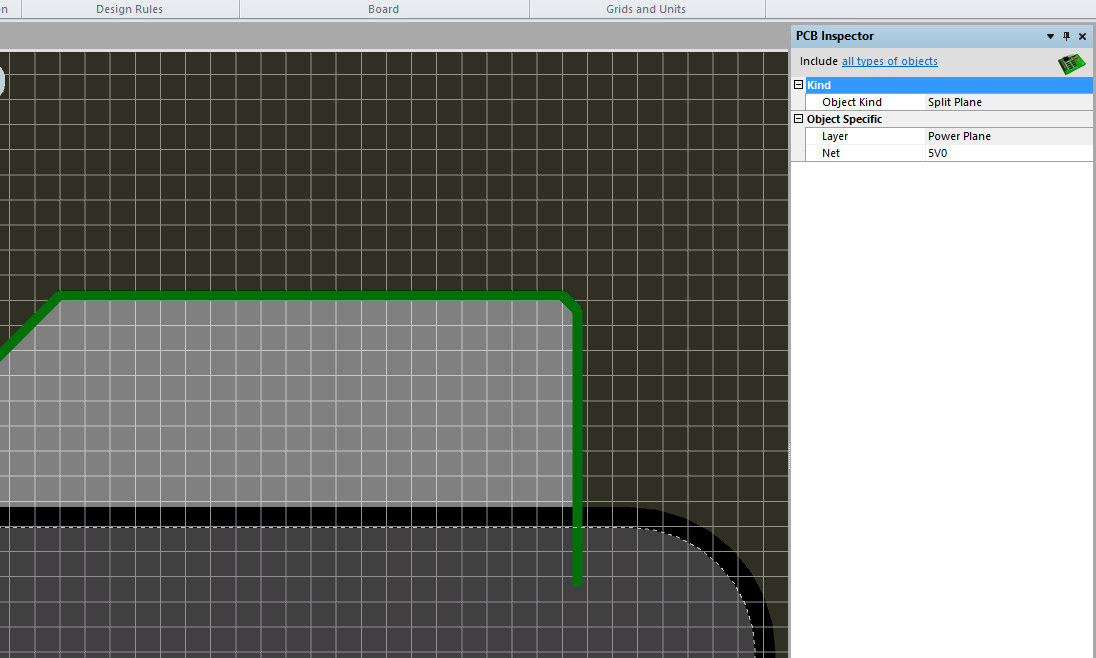
I also need to make 3 separate polygons on the power plane which will have different net names.  The CS documentation doesn't cover this.  I was able to make 4 layer board in the layer stack manager - but no net names, and not a lot of options there.


anyone doing 4 or more layer boards in CS?

  • Cancel
  • mflux_gamble
    0 mflux_gamble over 8 years ago

    Found the net name under the object inspector.  You can use the Filters to help show which layer is selected.  Then if you click the Ground Plane tab at the bottom of the PCB editor, you can then click anywhere on the layer.  in the object inspector you'll get this:


    image

    • Cancel
    • Vote Up 0 Vote Down
    • Cancel
  • mflux_gamble
    0 mflux_gamble over 8 years ago in reply to mflux_gamble

    I am trying to split the power plane into 3 separate polygons.  I drew a polygon on the power plane layer, and the software crashed 3 times and sent reports, etc. out.

    • Cancel
    • Vote Up 0 Vote Down
    • Cancel
  • mflux_gamble
    0 mflux_gamble over 8 years ago in reply to mflux_gamble

    here i've drawn a fill on the power plane.  I am trying to asign it to a net name using the object inspector, or by double clicking on the fill and selecting a net name.  every time i select a net name it automatically puts the field back to 'No Net'


    image

    • Cancel
    • Vote Up 0 Vote Down
    • Cancel
  • mflux_gamble
    0 mflux_gamble over 8 years ago in reply to mflux_gamble

    Here i tried to put a polygon fill on a different layer, set it to a net name, then change the layer to internal power - CS crashed


    image

    • Cancel
    • Vote Up 0 Vote Down
    • Cancel
  • mflux_gamble
    0 mflux_gamble over 8 years ago in reply to mflux_gamble

    I've got it figured out.  you can draw a Line.  if it sections off a portion of the existing internal layer, it will cut the polygon.  you can then select a different Net Name if you click on the sectioned off polygon. Here the main layer is 3v, now this new sectioned portion is 5v.


    the documentation on this is non-existent, and its not too obvious.


    in addition to that, the software had many crashes using the PCB inspector and so on - not great.  but at least it seems i have it sorted for the time being.


    image

    • Cancel
    • Vote Up 0 Vote Down
    • Cancel
  • batuu
    0 batuu over 8 years ago in reply to mflux_gamble

    You finaly found the right usage. Altium Designer and CS have two different concepts of layers. Signal layers and plane layers. Signal layers show the expected behaviour like the bottom and top layers.

    Plane layers are a kind of inverse layer. You draw the areas where no copper should be. As you explored, you can draw line segments to build areas similar to polygons and assign net names to them.

    Usualy these areas are called split planes.

    CS documentation for asisigning nets to splite planes can be found here : Split Plane | Online Documentation for Altium Products and here : PCB | Online Documentation for Altium Products


    Further readings: Internal Plane Information | Online Documentation for Altium Products


    If you want do get a little deeper into the concept of split planes, take a look at the AD documentation here : Internal Power and Split Planes | Online Documentation for Altium Products

    • Cancel
    • Vote Up 0 Vote Down
    • Cancel
element14 Community

element14 is the first online community specifically for engineers. Connect with your peers and get expert answers to your questions.

  • Members
  • Learn
  • Technologies
  • Challenges & Projects
  • Products
  • Store
  • About Us
  • Feedback & Support
  • FAQs
  • Terms of Use
  • Privacy Policy
  • Legal and Copyright Notices
  • Sitemap
  • Cookies

An Avnet Company © 2025 Premier Farnell Limited. All Rights Reserved.

Premier Farnell Ltd, registered in England and Wales (no 00876412), registered office: Farnell House, Forge Lane, Leeds LS12 2NE.

ICP 备案号 10220084.

Follow element14

  • X
  • Facebook
  • linkedin
  • YouTube