element14 Community
element14 Community
    Register Log In
  • Site
  • Search
  • Log In Register
  • Community Hub
    Community Hub
    • What's New on element14
    • Feedback and Support
    • Benefits of Membership
    • Personal Blogs
    • Members Area
    • Achievement Levels
  • Learn
    Learn
    • Ask an Expert
    • eBooks
    • element14 presents
    • Learning Center
    • Tech Spotlight
    • STEM Academy
    • Webinars, Training and Events
    • Learning Groups
  • Technologies
    Technologies
    • 3D Printing
    • FPGA
    • Industrial Automation
    • Internet of Things
    • Power & Energy
    • Sensors
    • Technology Groups
  • Challenges & Projects
    Challenges & Projects
    • Design Challenges
    • element14 presents Projects
    • Project14
    • Arduino Projects
    • Raspberry Pi Projects
    • Project Groups
  • Products
    Products
    • Arduino
    • Avnet Boards Community
    • Dev Tools
    • Manufacturers
    • Multicomp Pro
    • Product Groups
    • Raspberry Pi
    • RoadTests & Reviews
  • Store
    Store
    • Visit Your Store
    • Choose another store...
      • Europe
      •  Austria (German)
      •  Belgium (Dutch, French)
      •  Bulgaria (Bulgarian)
      •  Czech Republic (Czech)
      •  Denmark (Danish)
      •  Estonia (Estonian)
      •  Finland (Finnish)
      •  France (French)
      •  Germany (German)
      •  Hungary (Hungarian)
      •  Ireland
      •  Israel
      •  Italy (Italian)
      •  Latvia (Latvian)
      •  
      •  Lithuania (Lithuanian)
      •  Netherlands (Dutch)
      •  Norway (Norwegian)
      •  Poland (Polish)
      •  Portugal (Portuguese)
      •  Romania (Romanian)
      •  Russia (Russian)
      •  Slovakia (Slovak)
      •  Slovenia (Slovenian)
      •  Spain (Spanish)
      •  Sweden (Swedish)
      •  Switzerland(German, French)
      •  Turkey (Turkish)
      •  United Kingdom
      • Asia Pacific
      •  Australia
      •  China
      •  Hong Kong
      •  India
      •  Korea (Korean)
      •  Malaysia
      •  New Zealand
      •  Philippines
      •  Singapore
      •  Taiwan
      •  Thailand (Thai)
      • Americas
      •  Brazil (Portuguese)
      •  Canada
      •  Mexico (Spanish)
      •  United States
      Can't find the country/region you're looking for? Visit our export site or find a local distributor.
  • Translate
  • Profile
  • Settings
Altium CircuitStudio
  • Products
  • Manufacturers
  • Altium CircuitStudio
  • More
  • Cancel
Altium CircuitStudio
Altium CircuitStudio Forum Silk 2 SMask, or TopCu 2 SMask?
  • Blog
  • Forum
  • Documents
  • Events
  • Polls
  • Members
  • Mentions
  • Sub-Groups
  • Tags
  • More
  • Cancel
  • New
Join Altium CircuitStudio to participate - click to join for free!
Actions
  • Share
  • More
  • Cancel
Forum Thread Details
  • State Verified Answer
  • Locked Locked
  • Replies 5 replies
  • Subscribers 86 subscribers
  • Views 566 views
  • Users 0 members are here
  • drc
  • bug
  • ss2sm
Related
This discussion has been locked.
You can no longer post new replies to this discussion. If you have a question you can start a new discussion

Silk 2 SMask, or TopCu 2 SMask?

tlc8126
tlc8126 over 8 years ago

Running thru the Tutorial for the 2nd time, I noticed this - a DRC violation that shows one thing, but is caught by a different design rule:

image

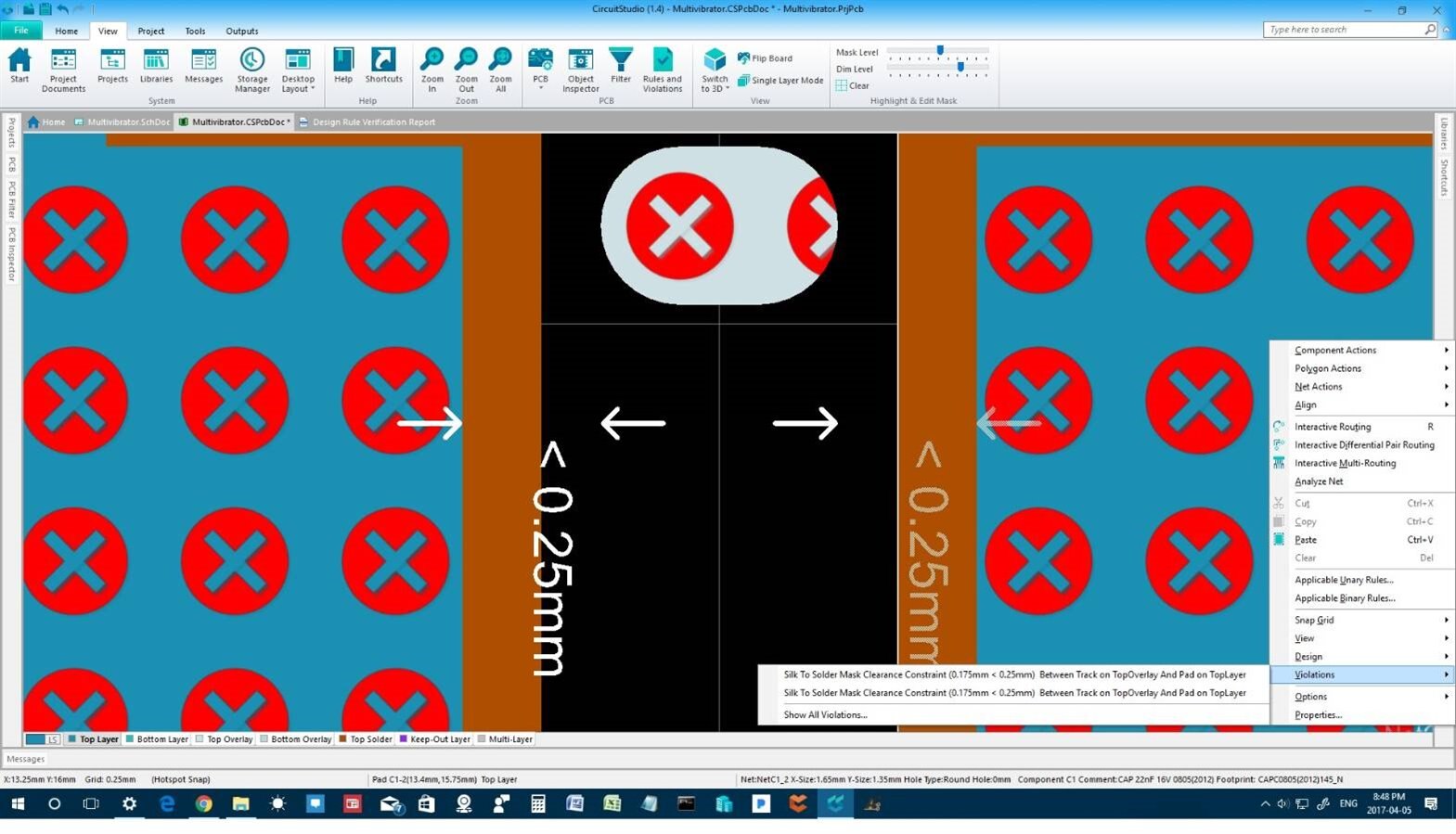
This looks like a Copper to Silkscreen, not Soldermask to Silkscreen violation. Is this a bug?


Regards,

Thomas

  • Cancel
  • tlc8126
    0 tlc8126 over 8 years ago

    Sorry, that title should read, "Silk 2 SMask, or Silk 2 TopCu".


    - Thomas

    • Cancel
    • Vote Up 0 Vote Down
    • Cancel
  • jamesharrimanaltium
    0 jamesharrimanaltium over 8 years ago in reply to tlc8126

    Hi Thomas,


    Please check your Silk To Solder mask Clearance design rule, if it is set to Clearance Checking Mode: Check Clearance to Exposed Copper. If so, then I think it's working correctly. If I'm not understanding this correctly, please attach the CSPcbDoc file.


    Best regards,


    James Harriman

    Altium

    • Cancel
    • Vote Up 0 Vote Down
    • Cancel
  • tlc8126
    0 tlc8126 over 8 years ago in reply to jamesharrimanaltium

    James,


    Thanks, totally missed that. Works perfectly when set right! (That's why I'm going thru the Tutorial once more to make sure I don't miss these sorts of things.)


    Regards,

    Thomas

    • Cancel
    • Vote Up 0 Vote Down
    • Cancel
  • tlc8126
    0 tlc8126 over 8 years ago in reply to jamesharrimanaltium

    James,


    Just one more note:  Neither the Tutorial or Documentation under PCB Design Rules, Manufacturing Rules mention this, and the Documentation for Manufacturing Rules is totally not there (it's blank). Can we see this completed any time soon? (I've noticed a number of Documentation pages just not completed, dated as having been created last year.) I'm still learning the software and rely a lot on the Documentation.


    Regards,

    Thomas


    P.S. I seriously thought that a Silkscreen to Solder Mask Clearance Constraint DRC would simply check just that - Silkscreen to Solder Mask. I didn't know there was an option to allow for Silkscreen ink on the bare laminate, as would happen in some cases when selecting Silk to Exposed Copper, or for when inking Silkscreen on Solder Mask over a Copper plane. Thanks again!

    • Cancel
    • Vote Up 0 Vote Down
    • Cancel
  • jamesharrimanaltium
    0 jamesharrimanaltium over 8 years ago in reply to tlc8126

    Hi Thomas,


    Yes Manufacturing rules will need to be added, the product is currently ahead of the documentation.


    Understandable given its name that the rule wouldn't check exposed copper!    


    Best regards,


    James Harriman

    Altium

    • Cancel
    • Vote Up 0 Vote Down
    • Cancel
element14 Community

element14 is the first online community specifically for engineers. Connect with your peers and get expert answers to your questions.

  • Members
  • Learn
  • Technologies
  • Challenges & Projects
  • Products
  • Store
  • About Us
  • Feedback & Support
  • FAQs
  • Terms of Use
  • Privacy Policy
  • Legal and Copyright Notices
  • Sitemap
  • Cookies

An Avnet Company © 2025 Premier Farnell Limited. All Rights Reserved.

Premier Farnell Ltd, registered in England and Wales (no 00876412), registered office: Farnell House, Forge Lane, Leeds LS12 2NE.

ICP 备案号 10220084.

Follow element14

  • X
  • Facebook
  • linkedin
  • YouTube