element14 Community
element14 Community
    Register Log In
  • Site
  • Search
  • Log In Register
  • Community Hub
    Community Hub
    • What's New on element14
    • Feedback and Support
    • Benefits of Membership
    • Personal Blogs
    • Members Area
    • Achievement Levels
  • Learn
    Learn
    • Ask an Expert
    • eBooks
    • element14 presents
    • Learning Center
    • Tech Spotlight
    • STEM Academy
    • Webinars, Training and Events
    • Learning Groups
  • Technologies
    Technologies
    • 3D Printing
    • FPGA
    • Industrial Automation
    • Internet of Things
    • Power & Energy
    • Sensors
    • Technology Groups
  • Challenges & Projects
    Challenges & Projects
    • Design Challenges
    • element14 presents Projects
    • Project14
    • Arduino Projects
    • Raspberry Pi Projects
    • Project Groups
  • Products
    Products
    • Arduino
    • Avnet Boards Community
    • Dev Tools
    • Manufacturers
    • Multicomp Pro
    • Product Groups
    • Raspberry Pi
    • RoadTests & Reviews
  • Store
    Store
    • Visit Your Store
    • Choose another store...
      • Europe
      •  Austria (German)
      •  Belgium (Dutch, French)
      •  Bulgaria (Bulgarian)
      •  Czech Republic (Czech)
      •  Denmark (Danish)
      •  Estonia (Estonian)
      •  Finland (Finnish)
      •  France (French)
      •  Germany (German)
      •  Hungary (Hungarian)
      •  Ireland
      •  Israel
      •  Italy (Italian)
      •  Latvia (Latvian)
      •  
      •  Lithuania (Lithuanian)
      •  Netherlands (Dutch)
      •  Norway (Norwegian)
      •  Poland (Polish)
      •  Portugal (Portuguese)
      •  Romania (Romanian)
      •  Russia (Russian)
      •  Slovakia (Slovak)
      •  Slovenia (Slovenian)
      •  Spain (Spanish)
      •  Sweden (Swedish)
      •  Switzerland(German, French)
      •  Turkey (Turkish)
      •  United Kingdom
      • Asia Pacific
      •  Australia
      •  China
      •  Hong Kong
      •  India
      •  Korea (Korean)
      •  Malaysia
      •  New Zealand
      •  Philippines
      •  Singapore
      •  Taiwan
      •  Thailand (Thai)
      • Americas
      •  Brazil (Portuguese)
      •  Canada
      •  Mexico (Spanish)
      •  United States
      Can't find the country/region you're looking for? Visit our export site or find a local distributor.
  • Translate
  • Profile
  • Settings
Altium CircuitStudio
  • Products
  • Manufacturers
  • Altium CircuitStudio
  • More
  • Cancel
Altium CircuitStudio
Altium CircuitStudio Forum Unrouted net constraint error.
  • Blog
  • Forum
  • Documents
  • Events
  • Polls
  • Members
  • Mentions
  • Sub-Groups
  • Tags
  • More
  • Cancel
  • New
Join Altium CircuitStudio to participate - click to join for free!
Actions
  • Share
  • More
  • Cancel
Forum Thread Details
  • State Verified Answer
  • Locked Locked
  • Replies 16 replies
  • Subscribers 90 subscribers
  • Views 8686 views
  • Users 0 members are here
  • net
  • routing
Related
This discussion has been locked.
You can no longer post new replies to this discussion. If you have a question you can start a new discussion

Unrouted net constraint error.

yadhu22krish@gmail.com
yadhu22krish@gmail.com over 7 years ago

Eventhough I connected the nets, Its showing unrouted net constaint. What am I doing wrong here ?

image

  • Cancel

Top Replies

  • csiemer
    csiemer over 7 years ago +1 verified
    Taking a wild guess, I would think maybe you forgot to check the box to make them plated through holes?
  • yadhu22krish@gmail.com
    yadhu22krish@gmail.com over 7 years ago in reply to csiemer +1
    Thanks Colby Siemer...That was the issue..Solved it...
  • e14softwareuk
    0 e14softwareuk over 7 years ago

    Difficult to answer from a small screenshot, if you would like me to take a look at the design please email directly to me. The PCB file should be sufficient for starters.

    • Cancel
    • Vote Up 0 Vote Down
    • Cancel
  • yadhu22krish@gmail.com
    0 yadhu22krish@gmail.com over 7 years ago in reply to e14softwareuk

    Sorry I cant share the design files. image

    Is there anthing else I can share with you ?

    • Cancel
    • Vote Up 0 Vote Down
    • Cancel
  • e14softwareuk
    0 e14softwareuk over 7 years ago in reply to yadhu22krish@gmail.com

    Without seeing the design it's difficult to guess what is wrong.

    • Cancel
    • Vote Up 0 Vote Down
    • Cancel
  • adamwebber
    0 adamwebber over 7 years ago

    Looks like you have GND and GND12.  Those are two separate nets.  Show a screenshot of your schematics where you connected them together.

    • Cancel
    • Vote Up 0 Vote Down
    • Cancel
  • yadhu22krish@gmail.com
    0 yadhu22krish@gmail.com over 7 years ago in reply to adamwebber

    Hi james,


    image

    • Cancel
    • Vote Up 0 Vote Down
    • Cancel
  • jimku
    0 jimku over 7 years ago

    What is the complete error message? Particularly, what net is it saying that is un-routed?

    • Cancel
    • Vote Up 0 Vote Down
    • Cancel
  • adamwebber
    0 adamwebber over 7 years ago in reply to yadhu22krish@gmail.com

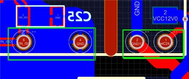
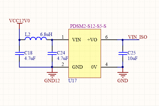
    This is quite a simple fix.  You have two separate ground nets.  Each one has a separate name.  GND12 and GND.  I see what you are trying to do.  But in order to physically connect the two nets together, you must do one of two things:


    1-Rename GND12 to GND.


    2-Phyiscally wire them together in your schematics.


    But both of these cases will give you a problem.  When you attempt to pour your polygon, it will pour both nets as one polygon.  I don't know exactly how to fix that.  You might just need to use a 0 ohm resistor to connect them together.  Or change the shape of your polygon pours.

    • Cancel
    • Vote Up 0 Vote Down
    • Cancel
  • yadhu22krish@gmail.com
    0 yadhu22krish@gmail.com over 7 years ago

    GND12 and GND are two seprate grounds. I want isolation between them.

    • Cancel
    • Vote Up 0 Vote Down
    • Cancel
  • yadhu22krish@gmail.com
    0 yadhu22krish@gmail.com over 7 years ago in reply to jimku

    All the nets: VIN_ISO, VCC12V0,GND and GND12.


    Error message is like all these nets are unconnected.

    • Cancel
    • Vote Up 0 Vote Down
    • Cancel
  • tarribred61
    0 tarribred61 over 7 years ago in reply to yadhu22krish@gmail.com

    Hi,


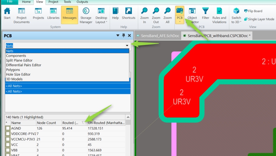
    This thread is confusing to me.  Can you describe the issue more clearly. Is there a report file you can look at that says what net is not fully routed?


    If you are getting an unrouted net constraint error then perhaps you can use the PCB tab to see what are the routed and unrouted lengths of the various nets on the design.  To do this select the PCB tab.


    1) from the tool ribbon pick the View tab then PCB to hide/unhide the PCB tab.

    2) From the drop down box choose Nets to show the nets in the design.

    3) you should then see a list of all the nets with their routed and unrouted lengths.


    You can sort the list of nets by clicking the columns headers to see the longest un-routed nets.  If you think all are connected and this shows a non-zero number in the un-routed net value then you can investigate or post that information.


    image

    • Cancel
    • Vote Up 0 Vote Down
    • Cancel
>
element14 Community

element14 is the first online community specifically for engineers. Connect with your peers and get expert answers to your questions.

  • Members
  • Learn
  • Technologies
  • Challenges & Projects
  • Products
  • Store
  • About Us
  • Feedback & Support
  • FAQs
  • Terms of Use
  • Privacy Policy
  • Legal and Copyright Notices
  • Sitemap
  • Cookies

An Avnet Company © 2025 Premier Farnell Limited. All Rights Reserved.

Premier Farnell Ltd, registered in England and Wales (no 00876412), registered office: Farnell House, Forge Lane, Leeds LS12 2NE.

ICP 备案号 10220084.

Follow element14

  • X
  • Facebook
  • linkedin
  • YouTube