element14 Community
element14 Community
    Register Log In
  • Site
  • Search
  • Log In Register
  • Community Hub
    Community Hub
    • What's New on element14
    • Feedback and Support
    • Benefits of Membership
    • Personal Blogs
    • Members Area
    • Achievement Levels
  • Learn
    Learn
    • Ask an Expert
    • eBooks
    • element14 presents
    • Learning Center
    • Tech Spotlight
    • STEM Academy
    • Webinars, Training and Events
    • Learning Groups
  • Technologies
    Technologies
    • 3D Printing
    • FPGA
    • Industrial Automation
    • Internet of Things
    • Power & Energy
    • Sensors
    • Technology Groups
  • Challenges & Projects
    Challenges & Projects
    • Design Challenges
    • element14 presents Projects
    • Project14
    • Arduino Projects
    • Raspberry Pi Projects
    • Project Groups
  • Products
    Products
    • Arduino
    • Avnet Boards Community
    • Dev Tools
    • Manufacturers
    • Multicomp Pro
    • Product Groups
    • Raspberry Pi
    • RoadTests & Reviews
  • About Us
  • Store
    Store
    • Visit Your Store
    • Choose another store...
      • Europe
      •  Austria (German)
      •  Belgium (Dutch, French)
      •  Bulgaria (Bulgarian)
      •  Czech Republic (Czech)
      •  Denmark (Danish)
      •  Estonia (Estonian)
      •  Finland (Finnish)
      •  France (French)
      •  Germany (German)
      •  Hungary (Hungarian)
      •  Ireland
      •  Israel
      •  Italy (Italian)
      •  Latvia (Latvian)
      •  
      •  Lithuania (Lithuanian)
      •  Netherlands (Dutch)
      •  Norway (Norwegian)
      •  Poland (Polish)
      •  Portugal (Portuguese)
      •  Romania (Romanian)
      •  Russia (Russian)
      •  Slovakia (Slovak)
      •  Slovenia (Slovenian)
      •  Spain (Spanish)
      •  Sweden (Swedish)
      •  Switzerland(German, French)
      •  Turkey (Turkish)
      •  United Kingdom
      • Asia Pacific
      •  Australia
      •  China
      •  Hong Kong
      •  India
      •  Korea (Korean)
      •  Malaysia
      •  New Zealand
      •  Philippines
      •  Singapore
      •  Taiwan
      •  Thailand (Thai)
      • Americas
      •  Brazil (Portuguese)
      •  Canada
      •  Mexico (Spanish)
      •  United States
      Can't find the country/region you're looking for? Visit our export site or find a local distributor.
  • Translate
  • Profile
  • Settings
Altium CircuitStudio
  • Products
  • Manufacturers
  • Altium CircuitStudio
  • More
  • Cancel
Altium CircuitStudio
Altium CircuitStudio Forum Schematic Symbols
  • Blog
  • Forum
  • Documents
  • Events
  • Polls
  • Members
  • Mentions
  • Sub-Groups
  • Tags
  • More
  • Cancel
  • New
Join Altium CircuitStudio to participate - click to join for free!
Actions
  • Share
  • More
  • Cancel
Forum Thread Details
  • State Suggested Answer
  • Locked Locked
  • Replies 3 replies
  • Answers 2 answers
  • Subscribers 90 subscribers
  • Views 1513 views
  • Users 0 members are here
  • frontpage
Related
This discussion has been locked.
You can no longer post new replies to this discussion. If you have a question you can start a new discussion

Schematic Symbols

kevinjbills@gmail.com
kevinjbills@gmail.com over 7 years ago

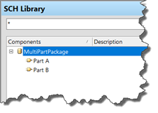
Is there a way to create schematic symbols that group pins of a large component into manageable sub-symbols for schematic entry?

  • Cancel

Top Replies

  • root2
    root2 over 7 years ago +1 suggested
    That is standard procedure with something like a dual and quad opamps so I guess you would draw sub symbols and name them for example IC1a, IC1b, IC1c, and so on, and place the appropriate pins accordingly…
  • csiemer
    csiemer over 7 years ago +1 suggested
    Also, to clarify the command you will use to do this. From the Schematic Library access the Tools tab of the ribbon and you will see the New Part and Remove Part buttons . New Part will add a secondary…
  • root2
    0 root2 over 7 years ago

    That is standard procedure with something like a dual and quad opamps so I guess you would draw sub symbols and name them for example IC1a, IC1b, IC1c, and so on, and place the appropriate pins accordingly.

    • Cancel
    • Vote Up +1 Vote Down
    • Cancel
  • e14softwareuk
    0 e14softwareuk over 7 years ago in reply to root2

    I would go along with Steve and also suggest dividing the symbol into sub-symbols. You can create as many (or few) sub-symbols as you like to make the design manageable.

    • Cancel
    • Vote Up 0 Vote Down
    • Cancel
  • csiemer
    0 csiemer over 7 years ago

    Also, to clarify the command you will use to do this.


    From the Schematic Library access the Tools tab of the ribbon and you will see the New Part and Remove Part buttons  .  New Part will add a secondary part to the symbol and will be given its own workspace to draw that part of the overall package.  This creates the A,B,C or 1,2,3 for the part so it can be placed throughout a schematic hierarchy easier, or to split by function.  On the SCH Library Panel your component should now show multiple parts

    imageimage

    Since each part has its own workspace, click on the Part you wish to edit here to access the workspace for that piece.


    They do as you would expect, they can be placed throughout the hierarchy, and when you go to update PCB they will all inform a single footprint's connections.


    I would not recommend taking something like a large connector(25+ pins) and splitting a component into individual pins for each part(i.e. a 25 pin connector split into 25 subparts), I have seen this done and it will cause a major performance drag within the schematic as the pin and part count increases due to the way we cache multi part components within the schematic.  Always better to have a good grouping of pins in the event of a large pin count item that needs to be split.  In the event you need to work with a large connector where you may be swapping pins around a lot, instead it is better to configure the connector for pin swapping, and label the nets.  This way you can swap pins as needed even in PCB, and synchronize the net changes back to the schematic for the connector.


    Also important to note, Remove Part will prompt you to make sure you actually want to remove the part, but the important bit is that this action cannot be undone, so do not delete part of a package unless you are sure you want it gone.


    Hope that helps

    • Cancel
    • Vote Up +1 Vote Down
    • Cancel
element14 Community

element14 is the first online community specifically for engineers. Connect with your peers and get expert answers to your questions.

  • Members
  • Learn
  • Technologies
  • Challenges & Projects
  • Products
  • Store
  • About Us
  • Feedback & Support
  • FAQs
  • Terms of Use
  • Privacy Policy
  • Legal and Copyright Notices
  • Sitemap
  • Cookies

An Avnet Company © 2025 Premier Farnell Limited. All Rights Reserved.

Premier Farnell Ltd, registered in England and Wales (no 00876412), registered office: Farnell House, Forge Lane, Leeds LS12 2NE.

ICP 备案号 10220084.

Follow element14

  • X
  • Facebook
  • linkedin
  • YouTube