element14 Community
element14 Community
    Register Log In
  • Site
  • Search
  • Log In Register
  • About Us
  • Community Hub
    Community Hub
    • What's New on element14
    • Feedback and Support
    • Benefits of Membership
    • Personal Blogs
    • Members Area
    • Achievement Levels
  • Learn
    Learn
    • Ask an Expert
    • eBooks
    • element14 presents
    • Learning Center
    • Tech Spotlight
    • STEM Academy
    • Webinars, Training and Events
    • Learning Groups
  • Technologies
    Technologies
    • 3D Printing
    • FPGA
    • Industrial Automation
    • Internet of Things
    • Power & Energy
    • Sensors
    • Technology Groups
  • Challenges & Projects
    Challenges & Projects
    • Design Challenges
    • element14 presents Projects
    • Project14
    • Arduino Projects
    • Raspberry Pi Projects
    • Project Groups
  • Products
    Products
    • Arduino
    • Avnet Boards Community
    • Dev Tools
    • Manufacturers
    • Multicomp Pro
    • Product Groups
    • Raspberry Pi
    • RoadTests & Reviews
  • Store
    Store
    • Visit Your Store
    • Choose another store...
      • Europe
      •  Austria (German)
      •  Belgium (Dutch, French)
      •  Bulgaria (Bulgarian)
      •  Czech Republic (Czech)
      •  Denmark (Danish)
      •  Estonia (Estonian)
      •  Finland (Finnish)
      •  France (French)
      •  Germany (German)
      •  Hungary (Hungarian)
      •  Ireland
      •  Israel
      •  Italy (Italian)
      •  Latvia (Latvian)
      •  
      •  Lithuania (Lithuanian)
      •  Netherlands (Dutch)
      •  Norway (Norwegian)
      •  Poland (Polish)
      •  Portugal (Portuguese)
      •  Romania (Romanian)
      •  Russia (Russian)
      •  Slovakia (Slovak)
      •  Slovenia (Slovenian)
      •  Spain (Spanish)
      •  Sweden (Swedish)
      •  Switzerland(German, French)
      •  Turkey (Turkish)
      •  United Kingdom
      • Asia Pacific
      •  Australia
      •  China
      •  Hong Kong
      •  India
      •  Korea (Korean)
      •  Malaysia
      •  New Zealand
      •  Philippines
      •  Singapore
      •  Taiwan
      •  Thailand (Thai)
      • Americas
      •  Brazil (Portuguese)
      •  Canada
      •  Mexico (Spanish)
      •  United States
      Can't find the country/region you're looking for? Visit our export site or find a local distributor.
  • Translate
  • Profile
  • Settings
Altium CircuitStudio
  • Products
  • Manufacturers
  • Altium CircuitStudio
  • More
  • Cancel
Altium CircuitStudio
Altium CircuitStudio Forum How to use Pad Class?
  • Blog
  • Forum
  • Documents
  • Events
  • Polls
  • Members
  • Mentions
  • Sub-Groups
  • Tags
  • More
  • Cancel
  • New
Join Altium CircuitStudio to participate - click to join for free!
Actions
  • Share
  • More
  • Cancel
Forum Thread Details
  • State Not Answered
  • Locked Locked
  • Replies 6 replies
  • Subscribers 88 subscribers
  • Views 6362 views
  • Users 0 members are here
  • pin
  • pad class
Related
This discussion has been locked.
You can no longer post new replies to this discussion. If you have a question you can start a new discussion

How to use Pad Class?

lamabrew
lamabrew over 7 years ago

I haven't turned up an explanation for this by searching (even in Designer). Apologies if I missed the obvious answer.


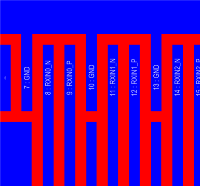
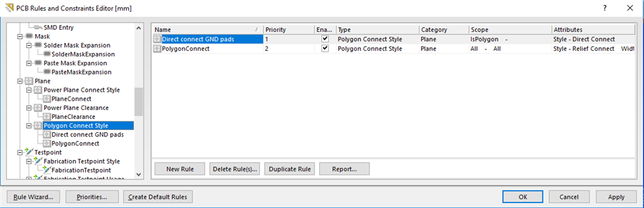
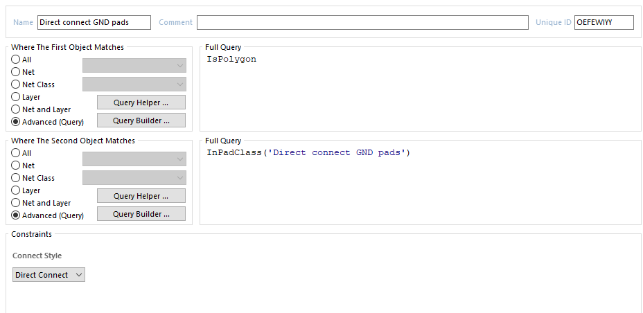
I want to assign a pad class to certain pins of a component so that the PCB tools knows how to connect it to a polygon. In this specific case the connector has multiple ground (shell) pins and I want them directly tied to the GND plane and not with thermal reliefs.


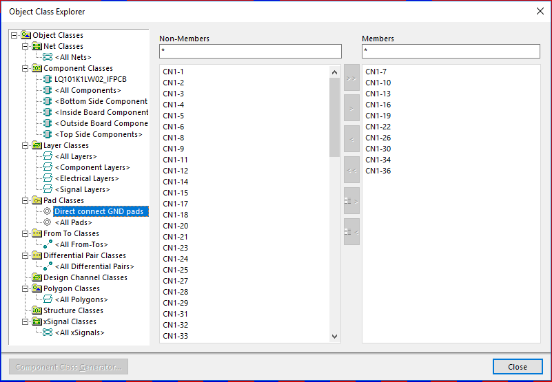
So far all I have been able to do is manually add the connector pins in PCB Class dialog. What I want to do is attach a Pad Class property to the PCB footprint in the library, or in the pin property for the part (I'm using integrated library and there is a 1:1 symbol to footprint correspondence).


I thought maybe after setting the pad class in PCB I could back annotate to the schematic and see what it was doing, but CS doesn't see adding a pad class as something that affects the schematic as it tells me there's nothing to do. I tried adding parameter to the pin for the component and updating in the forward direction but again CS says there's nothing to update.


There doesn't seem to be anything like the Directives->Net Class from the schematic side for setting Pad Class?

  • Cancel
Parents
  • csharp
    0 csharp over 7 years ago

    In my situation, Atium did not connect some ground pads using the thermal relief as I would expect. Direct connect connects them as I want, but I want to keep the relief connect for the rest of the polygon. Here shown are the pads with the relief connect rule:

    image


    I solved this by creating a specific pad class in the Object Class explorer: Design -> Classes -> Right click on Pad Classes -> Add Class


    And manually moved the pads that need the direct connect rule into this class:

    image


    Then I created a new polygon rule with higher priority (leaving the orignal rule that applies relief connect to the whole polygon).

    image


    The new rule uses "InPadClass" on "Where The Second Object Matches"

    image

    The result is that the specified ground pads have been connected using direct connect, but it hasn't affected the relief connect on the rest of the PCB:

    image


    FYI I am using Altium Designer 15.1.

    • Cancel
    • Vote Up 0 Vote Down
    • Cancel
Reply
  • csharp
    0 csharp over 7 years ago

    In my situation, Atium did not connect some ground pads using the thermal relief as I would expect. Direct connect connects them as I want, but I want to keep the relief connect for the rest of the polygon. Here shown are the pads with the relief connect rule:

    image


    I solved this by creating a specific pad class in the Object Class explorer: Design -> Classes -> Right click on Pad Classes -> Add Class


    And manually moved the pads that need the direct connect rule into this class:

    image


    Then I created a new polygon rule with higher priority (leaving the orignal rule that applies relief connect to the whole polygon).

    image


    The new rule uses "InPadClass" on "Where The Second Object Matches"

    image

    The result is that the specified ground pads have been connected using direct connect, but it hasn't affected the relief connect on the rest of the PCB:

    image


    FYI I am using Altium Designer 15.1.

    • Cancel
    • Vote Up 0 Vote Down
    • Cancel
Children
  • e14softwareuk
    0 e14softwareuk over 7 years ago in reply to csharp

    Hi Catherine, it is possible to use Pad Class rules in CircuitStudio and select specific pads just like with Designer. Unfortunately I still don't think there is a way to have library parts that have pads pre-assigned to a pad class so when loaded into a design they will automatically have the correct rules assigned.

    • Cancel
    • Vote Up 0 Vote Down
    • Cancel
  • lamabrew
    0 lamabrew over 7 years ago in reply to e14softwareuk

    Since this one has bubbled back up and I've been using CS for longer now...


    I'm kind of surprised that there's no concept of a "pad library," i.e. a pcblib like thing where I can define standard pad info (and associated Pad Class) and then place those in a component PCBLib instead of copy/pasting pads.  Maybe the use case for this doesn't come up that often, but I just spent time tweaking a bunch of parts that all have the same pad; got the Rev 1 boards back and wasn't happy with some solder issues.

    • Cancel
    • Vote Up 0 Vote Down
    • Cancel
element14 Community

element14 is the first online community specifically for engineers. Connect with your peers and get expert answers to your questions.

  • Members
  • Learn
  • Technologies
  • Challenges & Projects
  • Products
  • Store
  • About Us
  • Feedback & Support
  • FAQs
  • Terms of Use
  • Privacy Policy
  • Legal and Copyright Notices
  • Sitemap
  • Cookies

An Avnet Company © 2025 Premier Farnell Limited. All Rights Reserved.

Premier Farnell Ltd, registered in England and Wales (no 00876412), registered office: Farnell House, Forge Lane, Leeds LS12 2NE.

ICP 备案号 10220084.

Follow element14

  • X
  • Facebook
  • linkedin
  • YouTube