element14 Community
element14 Community
    Register Log In
  • Site
  • Search
  • Log In Register
  • About Us
  • Community Hub
    Community Hub
    • What's New on element14
    • Feedback and Support
    • Benefits of Membership
    • Personal Blogs
    • Members Area
    • Achievement Levels
  • Learn
    Learn
    • Ask an Expert
    • eBooks
    • element14 presents
    • Learning Center
    • Tech Spotlight
    • STEM Academy
    • Webinars, Training and Events
    • Learning Groups
  • Technologies
    Technologies
    • 3D Printing
    • FPGA
    • Industrial Automation
    • Internet of Things
    • Power & Energy
    • Sensors
    • Technology Groups
  • Challenges & Projects
    Challenges & Projects
    • Design Challenges
    • element14 presents Projects
    • Project14
    • Arduino Projects
    • Raspberry Pi Projects
    • Project Groups
  • Products
    Products
    • Arduino
    • Avnet Boards Community
    • Dev Tools
    • Manufacturers
    • Multicomp Pro
    • Product Groups
    • Raspberry Pi
    • RoadTests & Reviews
  • Store
    Store
    • Visit Your Store
    • Choose another store...
      • Europe
      •  Austria (German)
      •  Belgium (Dutch, French)
      •  Bulgaria (Bulgarian)
      •  Czech Republic (Czech)
      •  Denmark (Danish)
      •  Estonia (Estonian)
      •  Finland (Finnish)
      •  France (French)
      •  Germany (German)
      •  Hungary (Hungarian)
      •  Ireland
      •  Israel
      •  Italy (Italian)
      •  Latvia (Latvian)
      •  
      •  Lithuania (Lithuanian)
      •  Netherlands (Dutch)
      •  Norway (Norwegian)
      •  Poland (Polish)
      •  Portugal (Portuguese)
      •  Romania (Romanian)
      •  Russia (Russian)
      •  Slovakia (Slovak)
      •  Slovenia (Slovenian)
      •  Spain (Spanish)
      •  Sweden (Swedish)
      •  Switzerland(German, French)
      •  Turkey (Turkish)
      •  United Kingdom
      • Asia Pacific
      •  Australia
      •  China
      •  Hong Kong
      •  India
      •  Korea (Korean)
      •  Malaysia
      •  New Zealand
      •  Philippines
      •  Singapore
      •  Taiwan
      •  Thailand (Thai)
      • Americas
      •  Brazil (Portuguese)
      •  Canada
      •  Mexico (Spanish)
      •  United States
      Can't find the country/region you're looking for? Visit our export site or find a local distributor.
  • Translate
  • Profile
  • Settings
Altium CircuitStudio
  • Products
  • Manufacturers
  • Altium CircuitStudio
  • More
  • Cancel
Altium CircuitStudio
Altium CircuitStudio Forum Silkscreen Cutout
  • Blog
  • Forum
  • Documents
  • Events
  • Polls
  • Members
  • Mentions
  • Sub-Groups
  • Tags
  • More
  • Cancel
  • New
Join Altium CircuitStudio to participate - click to join for free!
Actions
  • Share
  • More
  • Cancel
Forum Thread Details
  • State Verified Answer
  • Locked Locked
  • Replies 10 replies
  • Answers 3 answers
  • Subscribers 88 subscribers
  • Views 3838 views
  • Users 0 members are here
  • frontpage
Related
This discussion has been locked.
You can no longer post new replies to this discussion. If you have a question you can start a new discussion

Silkscreen Cutout

r.gibson
r.gibson over 7 years ago

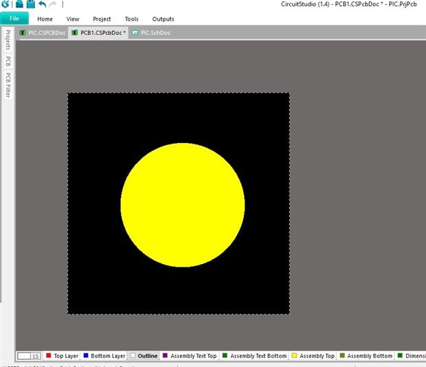
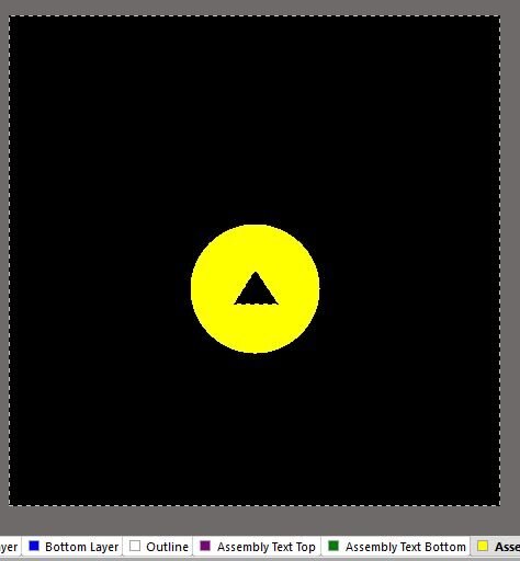
I am building Capacitive Touch buttons for my project and am overlaying each button with silkscreen. At the center of each silkscreen area I want to cut out an icon to represent the buttons function (ie. a negative image). I am having trouble figuring out an efficient way to do this. I tried using a Polygon Pour Cutout on the Top Overlay layer, but it doesn't seem to work.


The best way I have figured out at this point is to draw a 360° arc, with a thickness of about 1/3 of the radius of the circle that it is filling (such that the outer radius of the arc is the same radius as the button) which leaves a 2/3 unfilled circle within. Then using filled rectangles, add to the silkscreen layer until the shape I want is formed. This is a huge PITA when all I really want are basic geometric shapes that would normally be easy to accomplish as a "positive" image (ie. make the shape out of Silkscreen instead of taking away silkscreen). Am I missing something?

  • Cancel

Top Replies

  • mars01
    mars01 over 7 years ago in reply to r.gibson +1 suggested
    Hi, Regarding your point 3. " 3) Select Tools -> Convert -> "Create Polygon From Selected Primitives" It has been discusses before. The command is not in the GUI but you can access it by typing "convert…
  • mars01
    mars01 over 7 years ago in reply to r.gibson +1 suggested
    You have them both, although you've asked for Create Polygon ... For Pour and Unpour, select and then right click on a Polygon, under the Polygon Actions selection there is a list with many possible actions…
  • mars01
    mars01 over 7 years ago in reply to r.gibson +1 suggested
    Yes, the search function is context sensitive. Welcome to the world of CircuitStudio: everything is but not quite.You have to dig through it, the search function is the same as it is on Altium Designer…
Parents
  • e14softwareuk
    0 e14softwareuk over 7 years ago

    Polygon cutouts do work on the silk screen layer, you may need to right click on a polygon and Rebuild All to see the cutouts. Don't forget you can also have curved edges on polygons, just as when routing tracks use the SHIFT+SPACE to cycle through the available corner styles.

    • Cancel
    • Vote Up 0 Vote Down
    • Cancel
  • r.gibson
    0 r.gibson over 7 years ago in reply to e14softwareuk

    Ok...so I found a solution in Altium Designer...I'll see if I can reproduce it in Circuit Studio this evening:


    1) Select Place -> Full Circle

    2) Draw the circle

    3) Select Tools -> Convert -> "Create Polygon From Selected Primitives"

    4) Double-click somewhere in the center of the polygon to bring up the Polygon Pour menu

    5) Change Fill Mode to Solid and select OK

    6) Select Place -> "Polygon Pour Cutout"

    7) Draw negative image (to remove silk) inside the Polygon Pour (or outside, then drag in into place)

    8) Right click anywhere inside the Polygon Pour and select Polygon Actions -> "Repour All"

    • Cancel
    • Vote Up 0 Vote Down
    • Cancel
  • r.gibson
    0 r.gibson over 7 years ago in reply to r.gibson

    ...after trying the above method in CS, I'm beginning to realize how much simpler CS is than AD...as far as I can tell, there is no way to create a circular polygon pour in CS. Hopefully one of the e14 guys can come up with a solution...

    • Cancel
    • Vote Up 0 Vote Down
    • Cancel
  • mars01
    0 mars01 over 7 years ago in reply to r.gibson

    Hi,


    Regarding your point 3.

    "3) Select Tools -> Convert -> "Create Polygon From Selected Primitives"


    It has been discusses before. The command is not in the GUI but you can access it by typing "convert" keyword in the top right Search field.

    In the list of results that pop-up you'll find the command: "Convert -> Create Polygon From Selected Primitives"


    BTW: by Trial and Error you'll find other useful commands.


    Result:


    image

    • Cancel
    • Vote Up +1 Vote Down
    • Cancel
  • r.gibson
    0 r.gibson over 7 years ago in reply to mars01

    Marius, thank you for the tip! I hadn't played with the search field yet. I'll experiment with it in the future.


    However, you are slightly mistaken on the command...it is "Create Region From Selected Primitives" not "Create Polygon From Selected Primitives." Unfortunately there appears to be a significant difference as far as Altium is concerned when using the Polygon Pour Cutout (at least in Designer)...so unfortunately, it still doesn't help in this case. It is a good way to create a disk from a ring however. I previously used a pad for that...I like this method better.


    Also, I can't seem to find a "Pour" or "Repour" command in the search either...

    • Cancel
    • Vote Up 0 Vote Down
    • Cancel
  • mars01
    0 mars01 over 7 years ago in reply to r.gibson

    You have them both, although you've asked for Create Polygon ...


    image

    For Pour and Unpour, select and then right click on a Polygon, under the Polygon Actions selection there is a list with many possible actions, among them are those you mentioned.


    LE: If you want to access them through search field, type: "polygon".


    LLE: if I understood correctly, what you need is something like this:

    image

    • Cancel
    • Vote Up +1 Vote Down
    • Cancel
Reply
  • mars01
    0 mars01 over 7 years ago in reply to r.gibson

    You have them both, although you've asked for Create Polygon ...


    image

    For Pour and Unpour, select and then right click on a Polygon, under the Polygon Actions selection there is a list with many possible actions, among them are those you mentioned.


    LE: If you want to access them through search field, type: "polygon".


    LLE: if I understood correctly, what you need is something like this:

    image

    • Cancel
    • Vote Up +1 Vote Down
    • Cancel
Children
  • r.gibson
    0 r.gibson over 7 years ago in reply to mars01

    Ahhh, I think I see the problem...It appears to be context sensitive. The features that you showed are all available in the PCB editor, but NOT available in the PCB Library editor...I'm trying to create this as a footprint, so it's a reusable component that I can place as many times as I like. Any idea why those same commands aren't available in the footprint library editor? It seems to me that the two editors should share features...


    I was able to successfully reproduce the silkscreen that I want in the PCB editor, but even after copying and pasting the completed polygon back into the touch button in the library editor, it doesn't show up correctly...specifically it doesn't repour...I feel like I'm missing something here...why doesn't the PCB library editor allow me to do this?

    • Cancel
    • Vote Up 0 Vote Down
    • Cancel
  • mars01
    0 mars01 over 7 years ago in reply to r.gibson

    Yes, the search function is context sensitive.


    Welcome to the world of CircuitStudio: everything is but not quite.You have to dig through it, the search function is the same as it is on Altium Designer 18 so I think that CS served at some point as a testbed for different features. This search function is quite powerful, you can search for components, nets, built-in commands that are not exposed in GUI (yet, I hope). I advice you to have a look in the Altium Designer menu structure and try to search for the names of those functions. Some they might be in CS.


    You can build your custom silkscreen on a PCB file and then copy/paste everything in the PcbLib file. Like in picture below.

    As for why the polygons are not automatically repoured (although there is a reference there) it might be because CircuitStudio is not a completely finished product and we are all waiting anxiously for the next update that should solve all those problems. I understand from another forum, that one Altium support guy promised that now everything is on track and the delay in CS updates is due of the release of Altium Designer 18 which, understandable, took the focus of the programmer team. Which I sort of suspected all along.


    image

    • Cancel
    • Vote Up +1 Vote Down
    • Cancel
element14 Community

element14 is the first online community specifically for engineers. Connect with your peers and get expert answers to your questions.

  • Members
  • Learn
  • Technologies
  • Challenges & Projects
  • Products
  • Store
  • About Us
  • Feedback & Support
  • FAQs
  • Terms of Use
  • Privacy Policy
  • Legal and Copyright Notices
  • Sitemap
  • Cookies

An Avnet Company © 2025 Premier Farnell Limited. All Rights Reserved.

Premier Farnell Ltd, registered in England and Wales (no 00876412), registered office: Farnell House, Forge Lane, Leeds LS12 2NE.

ICP 备案号 10220084.

Follow element14

  • X
  • Facebook
  • linkedin
  • YouTube