Hello,
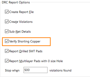
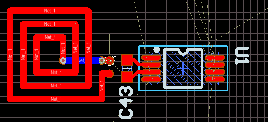
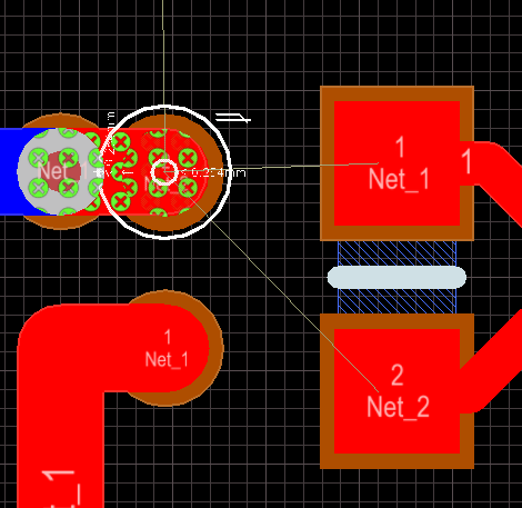
I am designing the PCB NFC antenna in my project. The problem which I have faced is that on the schematic I place two pins 1 , 2 for antenna , but since this a traces on the layout it treat entire trace as single net so not allow me to connect second end to the right output see below. Could you advice me what trick I should you to overcame this limitation?
Schematic

Layout
Thanks a lot in advance
Jacek