element14 Community
element14 Community
    Register Log In
  • Site
  • Search
  • Log In Register
  • Community Hub
    Community Hub
    • What's New on element14
    • Feedback and Support
    • Benefits of Membership
    • Personal Blogs
    • Members Area
    • Achievement Levels
  • Learn
    Learn
    • Ask an Expert
    • eBooks
    • element14 presents
    • Learning Center
    • Tech Spotlight
    • STEM Academy
    • Webinars, Training and Events
    • Learning Groups
  • Technologies
    Technologies
    • 3D Printing
    • FPGA
    • Industrial Automation
    • Internet of Things
    • Power & Energy
    • Sensors
    • Technology Groups
  • Challenges & Projects
    Challenges & Projects
    • Design Challenges
    • element14 presents Projects
    • Project14
    • Arduino Projects
    • Raspberry Pi Projects
    • Project Groups
  • Products
    Products
    • Arduino
    • Avnet & Tria Boards Community
    • Dev Tools
    • Manufacturers
    • Multicomp Pro
    • Product Groups
    • Raspberry Pi
    • RoadTests & Reviews
  • About Us
  • Store
    Store
    • Visit Your Store
    • Choose another store...
      • Europe
      •  Austria (German)
      •  Belgium (Dutch, French)
      •  Bulgaria (Bulgarian)
      •  Czech Republic (Czech)
      •  Denmark (Danish)
      •  Estonia (Estonian)
      •  Finland (Finnish)
      •  France (French)
      •  Germany (German)
      •  Hungary (Hungarian)
      •  Ireland
      •  Israel
      •  Italy (Italian)
      •  Latvia (Latvian)
      •  
      •  Lithuania (Lithuanian)
      •  Netherlands (Dutch)
      •  Norway (Norwegian)
      •  Poland (Polish)
      •  Portugal (Portuguese)
      •  Romania (Romanian)
      •  Russia (Russian)
      •  Slovakia (Slovak)
      •  Slovenia (Slovenian)
      •  Spain (Spanish)
      •  Sweden (Swedish)
      •  Switzerland(German, French)
      •  Turkey (Turkish)
      •  United Kingdom
      • Asia Pacific
      •  Australia
      •  China
      •  Hong Kong
      •  India
      • Japan
      •  Korea (Korean)
      •  Malaysia
      •  New Zealand
      •  Philippines
      •  Singapore
      •  Taiwan
      •  Thailand (Thai)
      • Vietnam
      • Americas
      •  Brazil (Portuguese)
      •  Canada
      •  Mexico (Spanish)
      •  United States
      Can't find the country/region you're looking for? Visit our export site or find a local distributor.
  • Translate
  • Profile
  • Settings
Altium CircuitStudio
  • Products
  • Manufacturers
  • Altium CircuitStudio
  • More
  • Cancel
Altium CircuitStudio
Altium CircuitStudio Forum Completed PCB shows what looks like an unrouted Net between 2 Pins off Separate Nets
  • Blog
  • Forum
  • Documents
  • Events
  • Polls
  • Members
  • Mentions
  • Sub-Groups
  • Tags
  • More
  • Cancel
  • New
Join Altium CircuitStudio to participate - click to join for free!
Actions
  • Share
  • More
  • Cancel
Forum Thread Details
  • State Not Answered
  • Locked Locked
  • Replies 4 replies
  • Subscribers 88 subscribers
  • Views 1178 views
  • Users 0 members are here
  • frontpage
Related
This discussion has been locked.
You can no longer post new replies to this discussion. If you have a question you can start a new discussion

Completed PCB shows what looks like an unrouted Net between 2 Pins off Separate Nets

pcat
pcat over 7 years ago

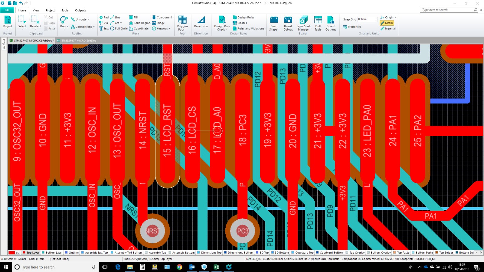
Hello I have just completed a PCB and when I zoomed in to check for a final inspection ,I found what looked like an in routed Net wire between 2 pins on my microcontroller.

When I hover over one of the pads a circle appears on the other pad but not vice versa.

If I hide all nets it goes away, there is no Net on the schematic joining these two pins that have their own Net labels that are on the PCB also.

I'm confused as to what it is trying to tell me.

I have a screen shot but don't know how to attached to this message.


Thanks


Paul

  • Cancel
  • e14softwareuk
    0 e14softwareuk over 7 years ago

    HI Paul, you should be able to copy and paste an image or use the image button to load an image file.image

    • Cancel
    • Vote Up 0 Vote Down
    • Cancel
  • pcat
    0 pcat over 7 years ago in reply to e14softwareuk

    Hi Peter, its between LCD_RST and LCD_A0

    No join on schematic no errors when compiling

    Thanks

    Paul

    image

    • Cancel
    • Vote Up 0 Vote Down
    • Cancel
  • e14softwareuk
    0 e14softwareuk over 7 years ago in reply to pcat

    A couple of things to try. First make sure your schematic and PCB components are in sync by checking Tools | Component Links in the PCB editor and that the netlists are in sync using Home | Project > Import Changes From {project}.


    1. Is there a fragment of track lurking under pin 17 (on any layer) that could be causing something to look like it is not routed?


    2. Check Tools | Netlist > Edit Nets... in the PCB editor - do the netlists for the two signals look correct.


    3. Reload the netlist by first running Tools | Netlist > Clear All Nets and then reloading using Home | Project > Import Changes From {project}.

    • Cancel
    • Vote Up 0 Vote Down
    • Cancel
  • pcat
    0 pcat over 7 years ago in reply to e14softwareuk

    Hi Peter,

    I always check the component links as it can get messed up when cutting and pasting in the schematic .

    However I didn't realise its safe to clear Nets after tracking then Import so learned something there. I was worried Hours of tracking would vanish  !


    But you were correct there was a tiny Blob of track on the top layer.

    Is there a method of hiding/turning off the components ? I have used this feature in other packages.

    I've played with the View/ PCB/Filter but cant find a way, I guess because the component footprint is on the Top Layer as per the Tracks


    Great support thanks

    • Cancel
    • Vote Up 0 Vote Down
    • Cancel
element14 Community

element14 is the first online community specifically for engineers. Connect with your peers and get expert answers to your questions.

  • Members
  • Learn
  • Technologies
  • Challenges & Projects
  • Products
  • Store
  • About Us
  • Feedback & Support
  • FAQs
  • Terms of Use
  • Privacy Policy
  • Legal and Copyright Notices
  • Sitemap
  • Cookies

An Avnet Company © 2026 Premier Farnell Limited. All Rights Reserved.

Premier Farnell Ltd, registered in England and Wales (no 00876412), registered office: Farnell House, Forge Lane, Leeds LS12 2NE.

ICP 备案号 10220084.

Follow element14

  • X
  • Facebook
  • linkedin
  • YouTube