element14 Community
element14 Community
    Register Log In
  • Site
  • Search
  • Log In Register
  • Community Hub
    Community Hub
    • What's New on element14
    • Feedback and Support
    • Benefits of Membership
    • Personal Blogs
    • Members Area
    • Achievement Levels
  • Learn
    Learn
    • Ask an Expert
    • eBooks
    • element14 presents
    • Learning Center
    • Tech Spotlight
    • STEM Academy
    • Webinars, Training and Events
    • Learning Groups
  • Technologies
    Technologies
    • 3D Printing
    • FPGA
    • Industrial Automation
    • Internet of Things
    • Power & Energy
    • Sensors
    • Technology Groups
  • Challenges & Projects
    Challenges & Projects
    • Design Challenges
    • element14 presents Projects
    • Project14
    • Arduino Projects
    • Raspberry Pi Projects
    • Project Groups
  • Products
    Products
    • Arduino
    • Avnet Boards Community
    • Dev Tools
    • Manufacturers
    • Multicomp Pro
    • Product Groups
    • Raspberry Pi
    • RoadTests & Reviews
  • About Us
  • Store
    Store
    • Visit Your Store
    • Choose another store...
      • Europe
      •  Austria (German)
      •  Belgium (Dutch, French)
      •  Bulgaria (Bulgarian)
      •  Czech Republic (Czech)
      •  Denmark (Danish)
      •  Estonia (Estonian)
      •  Finland (Finnish)
      •  France (French)
      •  Germany (German)
      •  Hungary (Hungarian)
      •  Ireland
      •  Israel
      •  Italy (Italian)
      •  Latvia (Latvian)
      •  
      •  Lithuania (Lithuanian)
      •  Netherlands (Dutch)
      •  Norway (Norwegian)
      •  Poland (Polish)
      •  Portugal (Portuguese)
      •  Romania (Romanian)
      •  Russia (Russian)
      •  Slovakia (Slovak)
      •  Slovenia (Slovenian)
      •  Spain (Spanish)
      •  Sweden (Swedish)
      •  Switzerland(German, French)
      •  Turkey (Turkish)
      •  United Kingdom
      • Asia Pacific
      •  Australia
      •  China
      •  Hong Kong
      •  India
      •  Korea (Korean)
      •  Malaysia
      •  New Zealand
      •  Philippines
      •  Singapore
      •  Taiwan
      •  Thailand (Thai)
      • Americas
      •  Brazil (Portuguese)
      •  Canada
      •  Mexico (Spanish)
      •  United States
      Can't find the country/region you're looking for? Visit our export site or find a local distributor.
  • Translate
  • Profile
  • Settings
Altium CircuitStudio
  • Products
  • Manufacturers
  • Altium CircuitStudio
  • More
  • Cancel
Altium CircuitStudio
Altium CircuitStudio Forum Question about Ground Planes in Circuit Stuido
  • Blog
  • Forum
  • Documents
  • Events
  • Polls
  • Members
  • Mentions
  • Sub-Groups
  • Tags
  • More
  • Cancel
  • New
Join Altium CircuitStudio to participate - click to join for free!
Actions
  • Share
  • More
  • Cancel
Forum Thread Details
  • State Suggested Answer
  • Locked Locked
  • Replies 9 replies
  • Answers 2 answers
  • Subscribers 89 subscribers
  • Views 2083 views
  • Users 0 members are here
  • frontpage
Related
This discussion has been locked.
You can no longer post new replies to this discussion. If you have a question you can start a new discussion

Question about Ground Planes in Circuit Stuido

alienjack
alienjack over 6 years ago

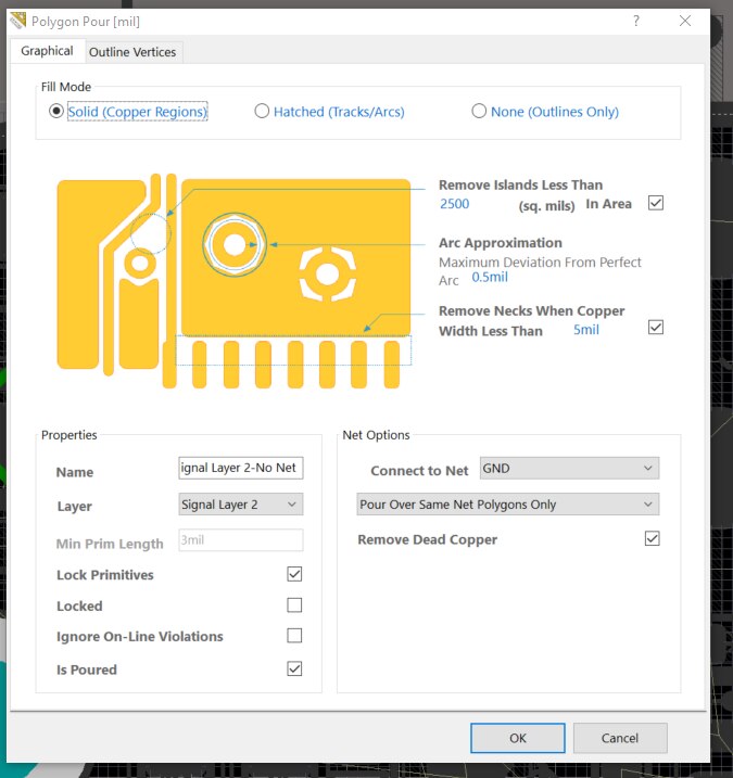
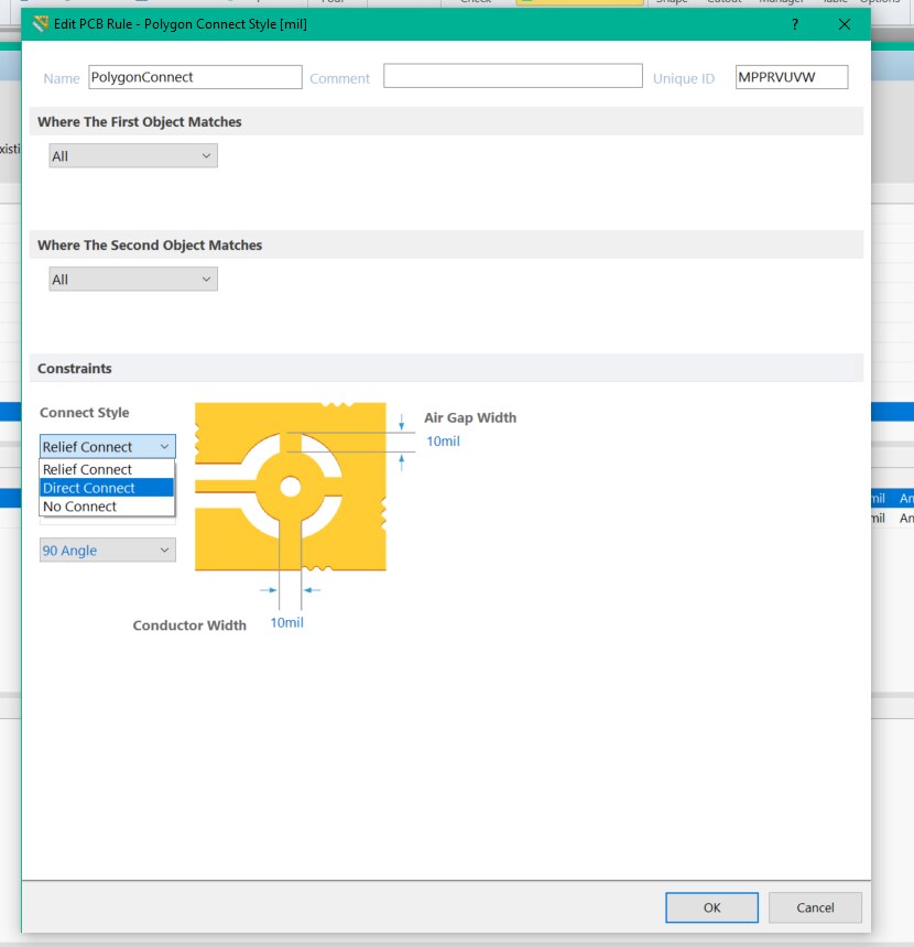
Hello, I am new to Circuit Studio. I have a few technical questions about the program that I can't seem to find answers for on line. The first one is... how do I connect a pad, either through hole or SM, to a ground plane?

  • Cancel

Top Replies

  • tarribred61
    tarribred61 over 6 years ago +1
    Hi, That is a pretty general and basic question. Have you searched for an gone through some of the tutorials? Circuitstudio has some and also some for Altium Designer might help you. Maybe start at this…
  • e14softwareuk
    e14softwareuk over 6 years ago in reply to alienjack +1 suggested
    Hi Jack. In addition to Thomas's suggestion I would also recommend watching the tutorial videos that are on this site if you are new to CircuitStudio and want to get up to speed quickly. Getting Started…
  • tarribred61
    0 tarribred61 over 6 years ago

    Hi,


    That is a pretty general and basic question. Have you searched for an gone through some of the tutorials?  Circuitstudio has some and also some for Altium Designer might help you.


    Maybe start at this link below or find some others....

    From Idea to Manufacture - Driving a PCB Design through CircuitStudio | Online Documentation for Altium Products


    Other sites and even other PCB design software may describe the basics


    When you are in the PCB design (as opposed to schematic design) you would use a via to connect an outer layer pad to a ground plane on an inner layer.  If you instead mean a ground flood on an outer layer then you would place a net to connect these.

    • Cancel
    • Vote Up +1 Vote Down
    • Cancel
  • alienjack
    0 alienjack over 6 years ago

    Hi Thomas. Thank you for your help. As I stated in my question, I am new to Circuit Studio, so I really appreciate you taking the time out to help me. I will research the site you gave me. How would I construct a net in the PCB design mode? What I need to do is to pour a GND plane on my bottom layer and open up all the pads that need to see ground to it so that they connect. I'm just not sure how to establish a net for a GND plane.

    • Cancel
    • Vote Up 0 Vote Down
    • Cancel
  • e14softwareuk
    0 e14softwareuk over 6 years ago in reply to alienjack

    Hi Jack.


    In addition to Thomas's suggestion I would also recommend watching the tutorial videos that are on this site if you are new to CircuitStudio and want to get up to speed quickly.

    Getting Started with CircuitStudio: Video Tutorial Series


    CircuitStudio works best when you start with a schematic design for your circuit that allows entry of all the parts and net connectivity. This is then used to generate the PCB which you can they layout and route. If you are trying to work on just a PCB then you will find it very difficult because you will need to go around manually assigning nets to pins which is harder than doing the same on a schematic.

    • Cancel
    • Vote Up +1 Vote Down
    • Cancel
  • tarribred61
    0 tarribred61 over 6 years ago in reply to alienjack

    See my reply on the other question you asked about PCB scoring.  I think the element14 videos for CircuitStudio will go along way to answer some of your questions and help minimize frustration.


    The basic answer to your question might be, once you define a copper pour area/shape on your layer you would configure it and assign a net name.  You might first draw the lines, arcs and such as primitives and then select them and use the Polygon Pour menu to define a Polygon Pour from the selected objects.


    Then select the pour shape and configure it as you want.  This will take some experimentation for you at first.

    image


    To tie the component pads to the copper pour (or ground flood) you would need to specify how to connect as part of the rules.  In that case, it would be the Polygon Connect Style type of rule.  You might want a relief connect or direct connect or you can instead place nets to manually make the connection.

    image

    • Cancel
    • Vote Up 0 Vote Down
    • Cancel
  • alienjack
    0 alienjack over 6 years ago in reply to e14softwareuk

    Hi Peter,


    Thank you for your input. I have watched the tutorial videos. There is a tutorial that has 11 videos in all and I watched them. They have helped me a lot and I am getting more familiar with Circuit Studio, but I didn't see where they mentioned connecting a pad directly to a ground plane or how to add a score line to a PCB board, so that you can separate it into two sections. But I will continue to watch the tutorials and search the forum for answers. Thank you again for helping me to get started.

    • Cancel
    • Vote Up 0 Vote Down
    • Cancel
  • alienjack
    0 alienjack over 6 years ago

    Hello Thomas and Peter. 


    I am having another issue with Circuit Studio that I hope you can help me with. The issue is with the Altium Content Vault. When I search for a part, in the vault explorer,  I use to get a folder that was titled “All Folders” and the part I was searching for was inside that folder. I would click on the folder, it would open and the part list would appear. For some reason, this folder no longer appears when I do a part search in the vault explorer. Now what I get is a folder that reads, “ Object reference not set to an instance of an object”. I click on the fold, but nothing happens. It doesn’t open. Please see the attached screen shot. Do you know what might be causing this issue and how I can get back to the folder that use to say “All Folders”, so that I can view the parts that I am searching for?


    image

    • Cancel
    • Vote Up 0 Vote Down
    • Cancel
  • tarribred61
    0 tarribred61 over 6 years ago in reply to alienjack

    Please see the several other related threads that have happened in the past week.  This seems to be a new issue that people are seeing.  We are waiting to hear from Altium on this.

    • Cancel
    • Vote Up 0 Vote Down
    • Cancel
  • alienjack
    0 alienjack over 6 years ago in reply to tarribred61

    Ok, thank you. It's very frustrating. It was working fine a few days ago then it started giving me issues the other day. Is there any thread that tells you how to correct the issue?

    • Cancel
    • Vote Up 0 Vote Down
    • Cancel
  • e14softwareuk
    0 e14softwareuk over 6 years ago in reply to alienjack

    We are waiting for Altium to investigate as the vault issue does seem to be affecting a number of people.

    • Cancel
    • Vote Up 0 Vote Down
    • Cancel
element14 Community

element14 is the first online community specifically for engineers. Connect with your peers and get expert answers to your questions.

  • Members
  • Learn
  • Technologies
  • Challenges & Projects
  • Products
  • Store
  • About Us
  • Feedback & Support
  • FAQs
  • Terms of Use
  • Privacy Policy
  • Legal and Copyright Notices
  • Sitemap
  • Cookies

An Avnet Company © 2025 Premier Farnell Limited. All Rights Reserved.

Premier Farnell Ltd, registered in England and Wales (no 00876412), registered office: Farnell House, Forge Lane, Leeds LS12 2NE.

ICP 备案号 10220084.

Follow element14

  • X
  • Facebook
  • linkedin
  • YouTube