element14 Community
element14 Community
    Register Log In
  • Site
  • Search
  • Log In Register
  • Community Hub
    Community Hub
    • What's New on element14
    • Feedback and Support
    • Benefits of Membership
    • Personal Blogs
    • Members Area
    • Achievement Levels
  • Learn
    Learn
    • Ask an Expert
    • eBooks
    • element14 presents
    • Learning Center
    • Tech Spotlight
    • STEM Academy
    • Webinars, Training and Events
    • Learning Groups
  • Technologies
    Technologies
    • 3D Printing
    • FPGA
    • Industrial Automation
    • Internet of Things
    • Power & Energy
    • Sensors
    • Technology Groups
  • Challenges & Projects
    Challenges & Projects
    • Design Challenges
    • element14 presents Projects
    • Project14
    • Arduino Projects
    • Raspberry Pi Projects
    • Project Groups
  • Products
    Products
    • Arduino
    • Avnet Boards Community
    • Dev Tools
    • Manufacturers
    • Multicomp Pro
    • Product Groups
    • Raspberry Pi
    • RoadTests & Reviews
  • Store
    Store
    • Visit Your Store
    • Choose another store...
      • Europe
      •  Austria (German)
      •  Belgium (Dutch, French)
      •  Bulgaria (Bulgarian)
      •  Czech Republic (Czech)
      •  Denmark (Danish)
      •  Estonia (Estonian)
      •  Finland (Finnish)
      •  France (French)
      •  Germany (German)
      •  Hungary (Hungarian)
      •  Ireland
      •  Israel
      •  Italy (Italian)
      •  Latvia (Latvian)
      •  
      •  Lithuania (Lithuanian)
      •  Netherlands (Dutch)
      •  Norway (Norwegian)
      •  Poland (Polish)
      •  Portugal (Portuguese)
      •  Romania (Romanian)
      •  Russia (Russian)
      •  Slovakia (Slovak)
      •  Slovenia (Slovenian)
      •  Spain (Spanish)
      •  Sweden (Swedish)
      •  Switzerland(German, French)
      •  Turkey (Turkish)
      •  United Kingdom
      • Asia Pacific
      •  Australia
      •  China
      •  Hong Kong
      •  India
      •  Korea (Korean)
      •  Malaysia
      •  New Zealand
      •  Philippines
      •  Singapore
      •  Taiwan
      •  Thailand (Thai)
      • Americas
      •  Brazil (Portuguese)
      •  Canada
      •  Mexico (Spanish)
      •  United States
      Can't find the country/region you're looking for? Visit our export site or find a local distributor.
  • Translate
  • Profile
  • Settings
Altium CircuitStudio
  • Products
  • Manufacturers
  • Altium CircuitStudio
  • More
  • Cancel
Altium CircuitStudio
Altium CircuitStudio Forum Board cutouts don't show in Gerbers, was Generating arcs for milling slots in Gerbers
  • Blog
  • Forum
  • Documents
  • Events
  • Polls
  • Members
  • Mentions
  • Sub-Groups
  • Tags
  • More
  • Cancel
  • New
Join Altium CircuitStudio to participate - click to join for free!
Actions
  • Share
  • More
  • Cancel
Forum Thread Details
  • State Verified Answer
  • Locked Locked
  • Replies 8 replies
  • Subscribers 88 subscribers
  • Views 3458 views
  • Users 0 members are here
  • cutout
  • round
  • milling
  • circular
Related
This discussion has been locked.
You can no longer post new replies to this discussion. If you have a question you can start a new discussion

Board cutouts don't show in Gerbers, was Generating arcs for milling slots in Gerbers

lamabrew
lamabrew over 5 years ago

For posterity, here is the original message.  Please see new message for an update/re-ask as to me this now seems like either a "bug" or a lack of explanation of how it's supposed to work, or both.

-------------------------------------------------------

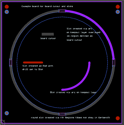
I must be overlooking some obvious step.  In the past I created (straight) milling slots by using elongated pads and that worked out well. But that doesn't work for arcs or other more complex shapes where I need to control the panelization (i.e. not simply defining the board shape in the gerber and let the board house do whatever it wants).


Using regions (created from primitives using the "hidden" Create region from primitives command) that I define as being board cutouts I get exactly what I want in the PCB editor. (slots are 2mm - default milling bit size, with tabs with 5-hole perfs).

image

I realize the board house will most likely want just the path for the router and not its actual shape, but I want to create gerbers with the routed slots so there's no confusion about inside vs. outside edge. As well as I like having the 3D view look like what I expect to get.


However when I create the Gerbers and NC drill files the slots don't show up in them when I examine them in my two viewers (GC-prevue and ZofzPCB).


Anyone have any guidance on creating slots like this?


Whatever board house gets used (most likely PCBWay) will have specific guidance (though I looked on their site and they don't for this case so if I do use them I'll obviously see what they want).  However at this point I just want to get a set of "generic" gerbers such that someone with a gerber viewer will see something that looks like the above rendering in CS's PCBEditor.


Thanks,

Brewster

  • Cancel

Top Replies

  • lamabrew
    lamabrew over 5 years ago in reply to frog +1
    @Frog I marked you as "correct" as you said it much more succinctly than my rambling question. Thank you for the help. However CS had other plans for me - yesterday one of the region board cutout slots…
  • frog
    frog over 5 years ago in reply to lamabrew +1
    As with so many things in life, we have to go with what we have. And despite its many imperfections, CS is what we have. Besides, there are more stuff-ups from the other side of the keyboard (mine at least…
  • frog
    0 frog over 5 years ago

    If you draw arcs on the 'outline' layer they will appear in the corresponding gerber.  Outline is a mechanical layer and may not be enabled by default.

    I've done this successfully on a number of PCBs, if in any doubt I'll send an image of what I expect the board to look like.  However, CS's idea of what the board outline is appears to be separate, so the 3D preview doesn't automatically pick them up.  I think that a better (although slightly more involved) method advocated by Peter Barnard involves creating board cutouts, although I never quite got the hang of creating arcs just the way I want them.


    Hope that helps.

    • Cancel
    • Vote Up 0 Vote Down
    • Cancel
  • lamabrew
    0 lamabrew over 5 years ago

    I made an example file (attached ) with regions defined as board cutouts arcs and rectangle), along with some arcs drawn on the keep-out layer, which is what the board house wants. There's also a slot made by adding a pad, which works fine for straight lines.

    image

    and CS renders a 3D view "as expected" (i.e. it ignore the keepout layer but the cutouts show):

    image

    But the generated Gerbers don't show the board cutouts in the 3 viewers I tried.  And they are not in the slot file, only the pad created slot is in that.


    The arcs do show in the keep out layer, and the board house will know what to do, etc.


    To me though this seems like a bug, i.e. what's the point of a "board cutout" if it doesn't end up in the gerber/NC drill data? Or is there a setting somewhere? (I've googled a bit but have not turned up anything)


    My workaround to get 3D renderings that are correct and gerbers the board house can use is to put keepout layer primitives that are positioned on top of the "board cutout" objects. That seems like a kluge for something that should be a somewhat common use case when dealing with non-square boards? If anyone has a better solution please let me know.


    Thanks,


    Brewster

    • Cancel
    • Vote Up 0 Vote Down
    • Cancel
  • lamabrew
    0 lamabrew over 5 years ago in reply to frog

    @Frog Thanks for looking at this.   I restated my problem, which is basically agreement with your observation that there's no simple way to get the 3D rendering to match, i.e. board cutouts don't show in the Gerbers (so what's the point of them?) and you can't say "make the primitives on layer X render as cutouts".


    So for now my workaround is use both overlaid on each other: board cutouts to make the 3D right and drawn primitives on a layer (GKO in my case for the board house) so they know what to do.

    • Cancel
    • Vote Up 0 Vote Down
    • Cancel
  • frog
    0 frog over 5 years ago in reply to lamabrew

    HI Brewster,

      Looking back through some previous designs I can't immediately find anything that quite matches what you're doing, but I think I've come to the same conclusion that creating a board cutout and a superimposed feature on the outline layer is the only way to get the 3D rendering and gerbers to match.  I've also generated STEP files for our CAD designer - this has also taken some experimentation to get everything across in a useful form.


    Cheers,

    Frog

    • Cancel
    • Vote Up 0 Vote Down
    • Cancel
  • clem57
    0 clem57 over 5 years ago

    Curious what is this going to be?

    • Cancel
    • Vote Up 0 Vote Down
    • Cancel
  • lamabrew
    0 lamabrew over 5 years ago in reply to frog

    @Frog  I marked you as "correct" as you said it much more succinctly than my rambling question. Thank you for the help.


    However CS had other plans for me - yesterday one of the region board cutout slots (the upper right one) disappeared from the generated output.  The hint I had was in PCBeditor it was no longer filled with the light grey color of the other three.  However its properties were identical - there's exactly one property that can be set, and it was set to "board cutout".


    After a lot of WTF I finally ending up deleting that region and copy/paste/rotate one of the three still working ones in to its place.


    CS did go through one of its "I'm going to crash after every 10th mouse click for the next hour" fits and it might have been during that the cutout broke. Lesson: even if you place a region that's a cutout it can still fail to show in the CS generated 3D views. Look for the magical grey filling image


    And it still leaves open the mystery of what's the point of "board cutouts" if they can't drive the Gerber data in some form...

    • Cancel
    • Vote Up +1 Vote Down
    • Cancel
  • lamabrew
    0 lamabrew over 5 years ago in reply to clem57

    @BB-Sphere It's an 8 channel microphone board with 8 RGB LEDs.  It's just a development/demonstration board that interfaces to some other hardware I have, ultimately it connects through an adapter board to (Analog Devices) A2B bus.

    • Cancel
    • Vote Up 0 Vote Down
    • Cancel
  • frog
    0 frog over 5 years ago in reply to lamabrew

    As with so many things in life, we have to go with what we have.  And despite its many imperfections, CS is what we have.  Besides, there are more stuff-ups from the other side of the keyboard (mine at least) so I shouldn't grumble too much.

    • Cancel
    • Vote Up +1 Vote Down
    • Cancel
element14 Community

element14 is the first online community specifically for engineers. Connect with your peers and get expert answers to your questions.

  • Members
  • Learn
  • Technologies
  • Challenges & Projects
  • Products
  • Store
  • About Us
  • Feedback & Support
  • FAQs
  • Terms of Use
  • Privacy Policy
  • Legal and Copyright Notices
  • Sitemap
  • Cookies

An Avnet Company © 2025 Premier Farnell Limited. All Rights Reserved.

Premier Farnell Ltd, registered in England and Wales (no 00876412), registered office: Farnell House, Forge Lane, Leeds LS12 2NE.

ICP 备案号 10220084.

Follow element14

  • X
  • Facebook
  • linkedin
  • YouTube