element14 Community
element14 Community
    Register Log In
  • Site
  • Search
  • Log In Register
  • About Us
  • Community Hub
    Community Hub
    • What's New on element14
    • Feedback and Support
    • Benefits of Membership
    • Personal Blogs
    • Members Area
    • Achievement Levels
  • Learn
    Learn
    • Ask an Expert
    • eBooks
    • element14 presents
    • Learning Center
    • Tech Spotlight
    • STEM Academy
    • Webinars, Training and Events
    • Learning Groups
  • Technologies
    Technologies
    • 3D Printing
    • FPGA
    • Industrial Automation
    • Internet of Things
    • Power & Energy
    • Sensors
    • Technology Groups
  • Challenges & Projects
    Challenges & Projects
    • Design Challenges
    • element14 presents Projects
    • Project14
    • Arduino Projects
    • Raspberry Pi Projects
    • Project Groups
  • Products
    Products
    • Arduino
    • Avnet Boards Community
    • Dev Tools
    • Manufacturers
    • Multicomp Pro
    • Product Groups
    • Raspberry Pi
    • RoadTests & Reviews
  • Store
    Store
    • Visit Your Store
    • Choose another store...
      • Europe
      •  Austria (German)
      •  Belgium (Dutch, French)
      •  Bulgaria (Bulgarian)
      •  Czech Republic (Czech)
      •  Denmark (Danish)
      •  Estonia (Estonian)
      •  Finland (Finnish)
      •  France (French)
      •  Germany (German)
      •  Hungary (Hungarian)
      •  Ireland
      •  Israel
      •  Italy (Italian)
      •  Latvia (Latvian)
      •  
      •  Lithuania (Lithuanian)
      •  Netherlands (Dutch)
      •  Norway (Norwegian)
      •  Poland (Polish)
      •  Portugal (Portuguese)
      •  Romania (Romanian)
      •  Russia (Russian)
      •  Slovakia (Slovak)
      •  Slovenia (Slovenian)
      •  Spain (Spanish)
      •  Sweden (Swedish)
      •  Switzerland(German, French)
      •  Turkey (Turkish)
      •  United Kingdom
      • Asia Pacific
      •  Australia
      •  China
      •  Hong Kong
      •  India
      •  Korea (Korean)
      •  Malaysia
      •  New Zealand
      •  Philippines
      •  Singapore
      •  Taiwan
      •  Thailand (Thai)
      • Americas
      •  Brazil (Portuguese)
      •  Canada
      •  Mexico (Spanish)
      •  United States
      Can't find the country/region you're looking for? Visit our export site or find a local distributor.
  • Translate
  • Profile
  • Settings
Altium CircuitStudio
  • Products
  • Manufacturers
  • Altium CircuitStudio
  • More
  • Cancel
Altium CircuitStudio
Altium CircuitStudio Forum Polygon pour issue/bug
  • Blog
  • Forum
  • Documents
  • Events
  • Polls
  • Members
  • Mentions
  • Sub-Groups
  • Tags
  • More
  • Cancel
  • New
Join Altium CircuitStudio to participate - click to join for free!
Actions
  • Share
  • More
  • Cancel
Forum Thread Details
  • State Verified Answer
  • Locked Locked
  • Replies 4 replies
  • Subscribers 89 subscribers
  • Views 6692 views
  • Users 0 members are here
  • frontpage
Related
This discussion has been locked.
You can no longer post new replies to this discussion. If you have a question you can start a new discussion

Polygon pour issue/bug

mo.abdol
mo.abdol over 5 years ago


I have been battling with a bug related to using the “Polygon pour” functionality for some time to no avail. The issue(s)/bug(s) is/are described below:


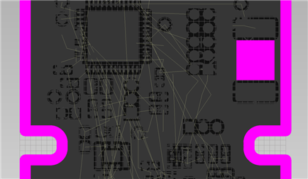
The board has four (4) layers, which are labeled as Top, L1, L2, and Bottom. All layers have been declared/assigned as “signal layer” except L1 which has been declared as an “internal plane” layer. Moreover, the board has a square shape with rounded corners.


Issue 1: When I try to carry out a polygon pour operation on the Top or Bottom layer, the filling algorithm/routine fills the entire (square) selected area. That is, it does not remove the dead copper which is outside the rounded corner area. Note that the check for removing the dead copper is enabled. But, the polygon pour operation works perfectly on the L1 layer which has been defined as an internal plane layer.


I have tried an alternative approach by defining the shape of the board on the Mechanical Layer, and then selecting the shape to do a “Define from selected objects”. This does not work properly either.


Issue 2: The L2 layer contains micro-vias that go from the L2 layer to the Bottom layer. Also, there are some through-vias that go from the Top layer to the Bottom layer. When I try to carry out a polygon pour operation on the L2 layer, the filling algorithm connects the poured section to the through-vias that do not belong to the same (selected net, i.e. GND net). But, the filling algorithm works as expected for all other regions including the micro-vias. It is as if the filling algorithm/routine has an issue with those items (through-vias) that don’t start/finish on this layer.


Any suggestions?


Thanks,


Mo


  • Cancel
Parents
  • tarribred61
    0 tarribred61 over 5 years ago

    Hey Mo,


    For number 1: I think Altium Designer works this way too and it is not a bug.  To get your layers to pour properly you either need to shape the areas exactly the way you want (not ideal) or use rules (this is preferred).  Maybe try what I describe below and see if it helps.


    Open Design Rules > Electrical > Clearance and make a new rule called Clearance_PolyTopLayer


    Set the first object match to layer and top layer.  Set the second object match to layer and Keep-Out Layer.


    If your keep-out layer is defined as the board outline with a thicker line such as 1mm then the top layer pour should pull back from the board edge by 0.5mm (1/2 the line width).  If the box for remove dead copper is checked then it should trim off the unconnected outer portions.  So basically you can put a big rectangular pour on the top layer that overhangs the PCB and it should trim off the off board copper and include a pull-back from the edge.


    I'm not sure about your #2 issue as I have not used blind vias with CircuitStudio.

    Screen shots for you:

    1st: here is top copper pour (red) and keepout (pink).  This PCB is unrouted as I'm in placement right now.


    image

    Here is single layer mode showing keepout and then copper only

    imageimage

    Here is my rule.  Full AD has more powerful rules but the process is basically the same.

    image

    Or you could instead define the rule to apply to polygons.

    image


    I confess to not being an expert at this (yet) though so some experimentation on your part is needed and maybe someone else can post a response.


    This link seems to describe some of the idea but with AD so it isn't exactly applicable.


    http://www.add.ece.ufl.edu/4924/docs/Altium_Polygon_Pour_Clearance.pdf

    • Cancel
    • Vote Up 0 Vote Down
    • Cancel
  • tarribred61
    0 tarribred61 over 5 years ago in reply to tarribred61

    Here is another older post that sort of applies to your question.


    https://www.element14.com/community/message/236084/l/questions-board-edge-polygon-clearance#236084

    • Cancel
    • Vote Up 0 Vote Down
    • Cancel
Reply
  • tarribred61
    0 tarribred61 over 5 years ago in reply to tarribred61

    Here is another older post that sort of applies to your question.


    https://www.element14.com/community/message/236084/l/questions-board-edge-polygon-clearance#236084

    • Cancel
    • Vote Up 0 Vote Down
    • Cancel
Children
No Data
element14 Community

element14 is the first online community specifically for engineers. Connect with your peers and get expert answers to your questions.

  • Members
  • Learn
  • Technologies
  • Challenges & Projects
  • Products
  • Store
  • About Us
  • Feedback & Support
  • FAQs
  • Terms of Use
  • Privacy Policy
  • Legal and Copyright Notices
  • Sitemap
  • Cookies

An Avnet Company © 2025 Premier Farnell Limited. All Rights Reserved.

Premier Farnell Ltd, registered in England and Wales (no 00876412), registered office: Farnell House, Forge Lane, Leeds LS12 2NE.

ICP 备案号 10220084.

Follow element14

  • X
  • Facebook
  • linkedin
  • YouTube