element14 Community
element14 Community
    Register Log In
  • Site
  • Search
  • Log In Register
  • About Us
  • Community Hub
    Community Hub
    • What's New on element14
    • Feedback and Support
    • Benefits of Membership
    • Personal Blogs
    • Members Area
    • Achievement Levels
  • Learn
    Learn
    • Ask an Expert
    • eBooks
    • element14 presents
    • Learning Center
    • Tech Spotlight
    • STEM Academy
    • Webinars, Training and Events
    • Learning Groups
  • Technologies
    Technologies
    • 3D Printing
    • FPGA
    • Industrial Automation
    • Internet of Things
    • Power & Energy
    • Sensors
    • Technology Groups
  • Challenges & Projects
    Challenges & Projects
    • Design Challenges
    • element14 presents Projects
    • Project14
    • Arduino Projects
    • Raspberry Pi Projects
    • Project Groups
  • Products
    Products
    • Arduino
    • Avnet Boards Community
    • Dev Tools
    • Manufacturers
    • Multicomp Pro
    • Product Groups
    • Raspberry Pi
    • RoadTests & Reviews
  • Store
    Store
    • Visit Your Store
    • Choose another store...
      • Europe
      •  Austria (German)
      •  Belgium (Dutch, French)
      •  Bulgaria (Bulgarian)
      •  Czech Republic (Czech)
      •  Denmark (Danish)
      •  Estonia (Estonian)
      •  Finland (Finnish)
      •  France (French)
      •  Germany (German)
      •  Hungary (Hungarian)
      •  Ireland
      •  Israel
      •  Italy (Italian)
      •  Latvia (Latvian)
      •  
      •  Lithuania (Lithuanian)
      •  Netherlands (Dutch)
      •  Norway (Norwegian)
      •  Poland (Polish)
      •  Portugal (Portuguese)
      •  Romania (Romanian)
      •  Russia (Russian)
      •  Slovakia (Slovak)
      •  Slovenia (Slovenian)
      •  Spain (Spanish)
      •  Sweden (Swedish)
      •  Switzerland(German, French)
      •  Turkey (Turkish)
      •  United Kingdom
      • Asia Pacific
      •  Australia
      •  China
      •  Hong Kong
      •  India
      •  Korea (Korean)
      •  Malaysia
      •  New Zealand
      •  Philippines
      •  Singapore
      •  Taiwan
      •  Thailand (Thai)
      • Americas
      •  Brazil (Portuguese)
      •  Canada
      •  Mexico (Spanish)
      •  United States
      Can't find the country/region you're looking for? Visit our export site or find a local distributor.
  • Translate
  • Profile
  • Settings
Altium CircuitStudio
  • Products
  • Manufacturers
  • Altium CircuitStudio
  • More
  • Cancel
Altium CircuitStudio
Altium CircuitStudio Forum Drill Symbol limit exceeded - CircuitStudio 1.5
  • Blog
  • Forum
  • Documents
  • Events
  • Polls
  • Members
  • Mentions
  • Sub-Groups
  • Tags
  • More
  • Cancel
  • New
Join Altium CircuitStudio to participate - click to join for free!
Actions
  • Share
  • More
  • Cancel
Forum Thread Details
  • State Suggested Answer
  • Locked Locked
  • Replies 5 replies
  • Answers 2 answers
  • Subscribers 93 subscribers
  • Views 2436 views
  • Users 0 members are here
  • circuitstudio 1.5
  • gerber error
  • frontpage
  • drill symbol
Related
This discussion has been locked.
You can no longer post new replies to this discussion. If you have a question you can start a new discussion

Drill Symbol limit exceeded - CircuitStudio 1.5

dabauza
dabauza over 5 years ago

Hi,


I´ve a problem when I generate gerber files from CircuitStudio 1.5 for a complex PCB.


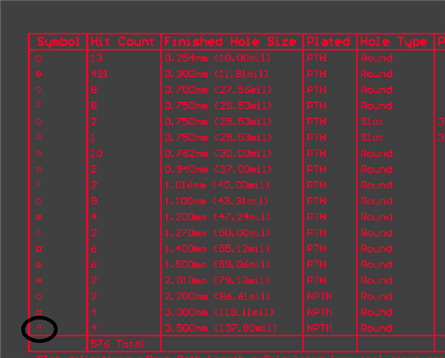
In the process to generate gerber files, the CircuitStudio launch the next message error:


"Drill Symbol limit exceeded. System will switch to letter generation"


I think that this message error appears in GD1 layer. This layer its necessary to poduce the PCB?


The PCB in question have 4 layers and multiple pads and vias.


I have review the gerver files with a gerber viewer and I think thats its correct. Only, in some drills appears letter to indicate a drill zone.


It thats any problem to send this files to PCB Factory? The factory can be produced correct PCBs from this files.


Thank you so much for the help

  • Cancel

Top Replies

  • mars01
    mars01 over 5 years ago +1 suggested
    In the Outputs section make sure that beside generating the Gerber files you generate also the NC drill files. The NC drill files holds the drills data. To make the PCB the manufacturer fab will need the…
  • lamabrew
    lamabrew over 5 years ago +1 suggested
    I've gotten that warning too. It seems harmless. OTOH when I look at the PCB hole report I see there's a lot of drill sizes that are "slightly" different and I try and reduce that, either by editing my…
  • mars01
    0 mars01 over 5 years ago

    In the Outputs section make sure that beside generating the Gerber files you generate also the NC drill files. The NC drill files holds the drills data.

    To make the PCB the manufacturer fab will need the following layers: Top Overlay, Top Solder, Top Layer, Bottom Overlay, Bottom Solder, Bottom Layer, Outline, Inner layers (if any), Mechanical layers (if you have some cutouts or the like) and the NC drill files (plated, non-plated holes).

    • Cancel
    • Vote Up +1 Vote Down
    • Cancel
  • lamabrew
    0 lamabrew over 5 years ago

    I've gotten that warning too. It seems harmless.  OTOH when I look at the PCB hole report I see there's a lot of drill sizes that are "slightly" different and I try and reduce that, either by editing my library footprints or just forcing holes to be a common size (i.e. 1.00, 1.01, and 1.03 mm can all be 1.0 mm) from inside the dialog/report. I assume the fab house probably already deals with that but I would rather send as clean of project as possible.  As well as sometimes some of the oddball ones I find turn out to be not quite right.


    YMMV

    Brewster

    • Cancel
    • Vote Up +1 Vote Down
    • Cancel
  • dabauza
    0 dabauza over 5 years ago

    Ok,Thank you for your answers.


    I'm going to try to use normalized drill to avoid error messages.

    • Cancel
    • Vote Up 0 Vote Down
    • Cancel
  • jack.chaney56
    0 jack.chaney56 over 5 years ago

    Is the drill change in question with a buried via?

    • Cancel
    • Vote Up 0 Vote Down
    • Cancel
  • isemi
    0 isemi over 3 years ago

    I just got this error as well. When generating the drill files circuit studio has a set of unique symbols it uses to represent the different drill sizes in the design. If you exceed the number of available symbols then CS it resorts to using letters as representation.  It doesn't seem to be a that big of a problem, but something to watch out for.


    image

    • Cancel
    • Vote Up 0 Vote Down
    • Cancel
element14 Community

element14 is the first online community specifically for engineers. Connect with your peers and get expert answers to your questions.

  • Members
  • Learn
  • Technologies
  • Challenges & Projects
  • Products
  • Store
  • About Us
  • Feedback & Support
  • FAQs
  • Terms of Use
  • Privacy Policy
  • Legal and Copyright Notices
  • Sitemap
  • Cookies

An Avnet Company © 2025 Premier Farnell Limited. All Rights Reserved.

Premier Farnell Ltd, registered in England and Wales (no 00876412), registered office: Farnell House, Forge Lane, Leeds LS12 2NE.

ICP 备案号 10220084.

Follow element14

  • X
  • Facebook
  • linkedin
  • YouTube