element14 Community
element14 Community
    Register Log In
  • Site
  • Search
  • Log In Register
  • Community Hub
    Community Hub
    • What's New on element14
    • Feedback and Support
    • Benefits of Membership
    • Personal Blogs
    • Members Area
    • Achievement Levels
  • Learn
    Learn
    • Ask an Expert
    • eBooks
    • element14 presents
    • Learning Center
    • Tech Spotlight
    • STEM Academy
    • Webinars, Training and Events
    • Learning Groups
  • Technologies
    Technologies
    • 3D Printing
    • FPGA
    • Industrial Automation
    • Internet of Things
    • Power & Energy
    • Sensors
    • Technology Groups
  • Challenges & Projects
    Challenges & Projects
    • Design Challenges
    • element14 presents Projects
    • Project14
    • Arduino Projects
    • Raspberry Pi Projects
    • Project Groups
  • Products
    Products
    • Arduino
    • Avnet & Tria Boards Community
    • Dev Tools
    • Manufacturers
    • Multicomp Pro
    • Product Groups
    • Raspberry Pi
    • RoadTests & Reviews
  • About Us
  • Store
    Store
    • Visit Your Store
    • Choose another store...
      • Europe
      •  Austria (German)
      •  Belgium (Dutch, French)
      •  Bulgaria (Bulgarian)
      •  Czech Republic (Czech)
      •  Denmark (Danish)
      •  Estonia (Estonian)
      •  Finland (Finnish)
      •  France (French)
      •  Germany (German)
      •  Hungary (Hungarian)
      •  Ireland
      •  Israel
      •  Italy (Italian)
      •  Latvia (Latvian)
      •  
      •  Lithuania (Lithuanian)
      •  Netherlands (Dutch)
      •  Norway (Norwegian)
      •  Poland (Polish)
      •  Portugal (Portuguese)
      •  Romania (Romanian)
      •  Russia (Russian)
      •  Slovakia (Slovak)
      •  Slovenia (Slovenian)
      •  Spain (Spanish)
      •  Sweden (Swedish)
      •  Switzerland(German, French)
      •  Turkey (Turkish)
      •  United Kingdom
      • Asia Pacific
      •  Australia
      •  China
      •  Hong Kong
      •  India
      • Japan
      •  Korea (Korean)
      •  Malaysia
      •  New Zealand
      •  Philippines
      •  Singapore
      •  Taiwan
      •  Thailand (Thai)
      • Vietnam
      • Americas
      •  Brazil (Portuguese)
      •  Canada
      •  Mexico (Spanish)
      •  United States
      Can't find the country/region you're looking for? Visit our export site or find a local distributor.
  • Translate
  • Profile
  • Settings
Altium CircuitStudio
  • Products
  • Manufacturers
  • Altium CircuitStudio
  • More
  • Cancel
Altium CircuitStudio
Altium CircuitStudio Forum Polygon not connecting to Pad
  • Blog
  • Forum
  • Documents
  • Events
  • Polls
  • Members
  • Mentions
  • Sub-Groups
  • Tags
  • More
  • Cancel
  • New
Join Altium CircuitStudio to participate - click to join for free!
Actions
  • Share
  • More
  • Cancel
Forum Thread Details
  • State Not Answered
  • Locked Locked
  • Replies 9 replies
  • Subscribers 91 subscribers
  • Views 5627 views
  • Users 0 members are here
  • relief
  • polygon pour
Related
This discussion has been locked.
You can no longer post new replies to this discussion. If you have a question you can start a new discussion

Polygon not connecting to Pad

dbemmann
dbemmann over 5 years ago

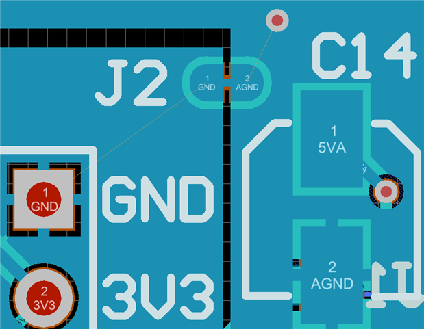
Strangely the pads of my component are not connecting to polygons of the same net. Why?


The component (J2 on the screenshot) is a self-designed solder-jumper defined as a net tie. On this PCB I want to use it to connect two ground planes (polygons with nets GND and AGND). As you can see, CircuitStudio doesn't connect the pads to the polygons.


Both polygons are set to "pour over all same net objects". I have two design rules for "polygon connect style":

Priority 1: first object = via, second object = all, connect style = direct connect

Priority 2: first object = all, second object = all, connect style = relief


You can both of them working on the other pads, but strangely not on the solder-jumper. On the other hand, these fine unrouted lines show that it should be connected. What am I doing wrong? Just for completeness, the component is built with 4 pads (two rounded ones overlapped by two rectangular ones). In any case there is enough room for relief lines.

image

  • Cancel
Parents
  • dbemmann
    0 dbemmann over 5 years ago

    A little update on this: I tried what happens when I remove the connecting track between the pads (in the component). Interestingly, then the pads connect to the polygons with relief, just as expected. But that's not a solution since the component is no longer a Net Tie now, and I cannot place that connecting track in the PCB editor either.

    • Cancel
    • Vote Up 0 Vote Down
    • Cancel
  • voltsandjolts
    0 voltsandjolts over 5 years ago in reply to dbemmann

    Ah, my net-tie footprints are just two rectangular pads which overlap slightly and that works.

    Having two pads with connecting track or fill, as I think you have, doesn't work.


    Don't think that gotcha is anywhere in the documentation!

    • Cancel
    • Vote Up 0 Vote Down
    • Cancel
  • dbemmann
    0 dbemmann over 5 years ago in reply to voltsandjolts

    I was not able to solve it. I tried unpouring and then placing tracks. That works, but still there is no connection between polygon and pad (other than the track). I tried removing the bridge track in the footprint and replacing it with a narrow pad. This doesn't solve it either. Having only two pads could maybe work, but there is no available pad geometry to make a usable solder jumper out of two pads (i.e. one that can easily be re-closed by soldering after the bridge has been cut).


    My workaround for now is to connect to the polygons with tracks. I'm not that happy because unless I connect these tracks to another object, CS tends to remove them sometimes.

    • Cancel
    • Vote Up 0 Vote Down
    • Cancel
Reply
  • dbemmann
    0 dbemmann over 5 years ago in reply to voltsandjolts

    I was not able to solve it. I tried unpouring and then placing tracks. That works, but still there is no connection between polygon and pad (other than the track). I tried removing the bridge track in the footprint and replacing it with a narrow pad. This doesn't solve it either. Having only two pads could maybe work, but there is no available pad geometry to make a usable solder jumper out of two pads (i.e. one that can easily be re-closed by soldering after the bridge has been cut).


    My workaround for now is to connect to the polygons with tracks. I'm not that happy because unless I connect these tracks to another object, CS tends to remove them sometimes.

    • Cancel
    • Vote Up 0 Vote Down
    • Cancel
Children
  • voltsandjolts
    0 voltsandjolts over 5 years ago in reply to dbemmann

    OK, I think you want a net-tie footprint that leaves the option of cutting the net-tie (for measuring current perhaps) and using a solder bridge repair.

    My preference for that is to use two seperate footprints.

    I have test points on each net which are large enough for soldering wires (current measurement) or a link (repair).

    The net-tie is a seperate footprint (just two overlapping pads) which can be cut.

    Overlay the net-tie and jumper if you like, with appropriate rule to ignore collision.


    image

    • Cancel
    • Vote Up 0 Vote Down
    • Cancel
element14 Community

element14 is the first online community specifically for engineers. Connect with your peers and get expert answers to your questions.

  • Members
  • Learn
  • Technologies
  • Challenges & Projects
  • Products
  • Store
  • About Us
  • Feedback & Support
  • FAQs
  • Terms of Use
  • Privacy Policy
  • Legal and Copyright Notices
  • Sitemap
  • Cookies

An Avnet Company © 2026 Premier Farnell Limited. All Rights Reserved.

Premier Farnell Ltd, registered in England and Wales (no 00876412), registered office: Farnell House, Forge Lane, Leeds LS12 2NE.

ICP 备案号 10220084.

Follow element14

  • X
  • Facebook
  • linkedin
  • YouTube