Strangely the pads of my component are not connecting to polygons of the same net. Why?
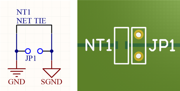
The component (J2 on the screenshot) is a self-designed solder-jumper defined as a net tie. On this PCB I want to use it to connect two ground planes (polygons with nets GND and AGND). As you can see, CircuitStudio doesn't connect the pads to the polygons.
Both polygons are set to "pour over all same net objects". I have two design rules for "polygon connect style":
Priority 1: first object = via, second object = all, connect style = direct connect
Priority 2: first object = all, second object = all, connect style = relief
You can both of them working on the other pads, but strangely not on the solder-jumper. On the other hand, these fine unrouted lines show that it should be connected. What am I doing wrong? Just for completeness, the component is built with 4 pads (two rounded ones overlapped by two rectangular ones). In any case there is enough room for relief lines.


