element14 Community
element14 Community
    Register Log In
  • Site
  • Search
  • Log In Register
  • About Us
  • Community Hub
    Community Hub
    • What's New on element14
    • Feedback and Support
    • Benefits of Membership
    • Personal Blogs
    • Members Area
    • Achievement Levels
  • Learn
    Learn
    • Ask an Expert
    • eBooks
    • element14 presents
    • Learning Center
    • Tech Spotlight
    • STEM Academy
    • Webinars, Training and Events
    • Learning Groups
  • Technologies
    Technologies
    • 3D Printing
    • FPGA
    • Industrial Automation
    • Internet of Things
    • Power & Energy
    • Sensors
    • Technology Groups
  • Challenges & Projects
    Challenges & Projects
    • Design Challenges
    • element14 presents Projects
    • Project14
    • Arduino Projects
    • Raspberry Pi Projects
    • Project Groups
  • Products
    Products
    • Arduino
    • Avnet Boards Community
    • Dev Tools
    • Manufacturers
    • Multicomp Pro
    • Product Groups
    • Raspberry Pi
    • RoadTests & Reviews
  • Store
    Store
    • Visit Your Store
    • Choose another store...
      • Europe
      •  Austria (German)
      •  Belgium (Dutch, French)
      •  Bulgaria (Bulgarian)
      •  Czech Republic (Czech)
      •  Denmark (Danish)
      •  Estonia (Estonian)
      •  Finland (Finnish)
      •  France (French)
      •  Germany (German)
      •  Hungary (Hungarian)
      •  Ireland
      •  Israel
      •  Italy (Italian)
      •  Latvia (Latvian)
      •  
      •  Lithuania (Lithuanian)
      •  Netherlands (Dutch)
      •  Norway (Norwegian)
      •  Poland (Polish)
      •  Portugal (Portuguese)
      •  Romania (Romanian)
      •  Russia (Russian)
      •  Slovakia (Slovak)
      •  Slovenia (Slovenian)
      •  Spain (Spanish)
      •  Sweden (Swedish)
      •  Switzerland(German, French)
      •  Turkey (Turkish)
      •  United Kingdom
      • Asia Pacific
      •  Australia
      •  China
      •  Hong Kong
      •  India
      •  Korea (Korean)
      •  Malaysia
      •  New Zealand
      •  Philippines
      •  Singapore
      •  Taiwan
      •  Thailand (Thai)
      • Americas
      •  Brazil (Portuguese)
      •  Canada
      •  Mexico (Spanish)
      •  United States
      Can't find the country/region you're looking for? Visit our export site or find a local distributor.
  • Translate
  • Profile
  • Settings
Altium CircuitStudio
  • Products
  • Manufacturers
  • Altium CircuitStudio
  • More
  • Cancel
Altium CircuitStudio
Altium CircuitStudio Forum Error with routing via style design rule
  • Blog
  • Forum
  • Documents
  • Events
  • Polls
  • Members
  • Mentions
  • Sub-Groups
  • Tags
  • More
  • Cancel
  • New
Join Altium CircuitStudio to participate - click to join for free!
Actions
  • Share
  • More
  • Cancel
Forum Thread Details
  • State Not Answered
  • Locked Locked
  • Replies 2 replies
  • Subscribers 89 subscribers
  • Views 1754 views
  • Users 0 members are here
Related
This discussion has been locked.
You can no longer post new replies to this discussion. If you have a question you can start a new discussion

Error with routing via style design rule

julach
julach over 4 years ago

Hello everyone,


I would like to define different routing via styles for BGA routing.

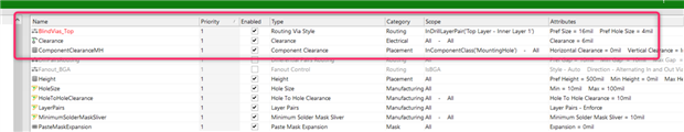
I would like to create rule for multi-layer via, and for top layer to layer 1.


In the layer stack manager/ drill pairs, I have the different drill pairs I can use.

image


And when I go to the design rules / routing / routing via style and I try to create the rule, I have a pop-up error saying "some rules have incorrect definitions". When I hover the rule, I see "Expression1 invalid".

image


Did I miss something for doing this ? Would someone know why I have the error while when I try with a net name, it works.


Thank you,

Justine

  • Cancel
Parents
  • julach
    0 julach over 4 years ago

    Anybody has the same issue ?

    • Cancel
    • Vote Up 0 Vote Down
    • Cancel
  • tarribred61
    0 tarribred61 over 4 years ago in reply to julach

    In CircuitStudio the routing via style is intended more for declaring a via size limit specially for high power nets (example AC-mains) where you want certain nets to enforce large vias and pads to handle the current/power.  Then you would put those nets in a net class and make a rule to prevent making the vias too small.  Similarly, you would define a net class for high thermal nets and then make a polygon connect style rule for direct connection.


    In your case, I would ask yourself if you really need a separate routing via style rule for blind or buried vias?  I understand that, for example, you might want to allow special rules for blind microvias for a multilayer build up with laser drilled holes on outer layers to adjacent inner layers.  Or maybe you would want to allow smaller holes on the inner layers buried vias since the core is thin and still have a rule that enforces min drill size on fully through hole vias.  That kind of sophisticated high density interconnect is where CircuitStudio begins to be crippled vs Altium Designer.  As you stated, you want to allow small blind vias for the BGA but presumably disallow small vias for others.


    Sadly, I'm not sure there is a good solution.  You should possibly define a net class and put the certain BGA nets into it.  Then base the rule on the net class.  I agree, these drill pair selections warning/error in the rules definitions should not be there if they truly generate invalid rules.


    Summary: these rules don't work completely CircuitStudio like they do on Altium Designer.  And there are bugs in menu selections.  The rules wizard is interesting and frustrating to play with as it shows some of the things you cannot do in CS that can be done in AD.


    But this brings up an interesting thing to try in the new release beta version and I think I'll have to see about it sometime this week.


    So, that all said, I worked with a sandbox board I have, and then made a rule based on drill pair to set the maximum hole size on a blind top to inner1 layer via to 8mil.  It says the rule selection criteria are invalid but I ignored the warning.  It did correctly find the violation if I made the via hole larger than 8 mil. and also if I made the pad violate the pad size for the via drill pair.  So, you might experiment with this a bit and let us know if warning it gives is the bug and the selection of drill pairs works or if the drill pairs based rules don't work.


    The report for rules gives me this. Says the scope is InDrillLayerPair('TopLayer - Inner Layer1'); that seems correct.

    image


    Thanks in advance for helping us understand this better.

    • Cancel
    • Vote Up 0 Vote Down
    • Cancel
Reply
  • tarribred61
    0 tarribred61 over 4 years ago in reply to julach

    In CircuitStudio the routing via style is intended more for declaring a via size limit specially for high power nets (example AC-mains) where you want certain nets to enforce large vias and pads to handle the current/power.  Then you would put those nets in a net class and make a rule to prevent making the vias too small.  Similarly, you would define a net class for high thermal nets and then make a polygon connect style rule for direct connection.


    In your case, I would ask yourself if you really need a separate routing via style rule for blind or buried vias?  I understand that, for example, you might want to allow special rules for blind microvias for a multilayer build up with laser drilled holes on outer layers to adjacent inner layers.  Or maybe you would want to allow smaller holes on the inner layers buried vias since the core is thin and still have a rule that enforces min drill size on fully through hole vias.  That kind of sophisticated high density interconnect is where CircuitStudio begins to be crippled vs Altium Designer.  As you stated, you want to allow small blind vias for the BGA but presumably disallow small vias for others.


    Sadly, I'm not sure there is a good solution.  You should possibly define a net class and put the certain BGA nets into it.  Then base the rule on the net class.  I agree, these drill pair selections warning/error in the rules definitions should not be there if they truly generate invalid rules.


    Summary: these rules don't work completely CircuitStudio like they do on Altium Designer.  And there are bugs in menu selections.  The rules wizard is interesting and frustrating to play with as it shows some of the things you cannot do in CS that can be done in AD.


    But this brings up an interesting thing to try in the new release beta version and I think I'll have to see about it sometime this week.


    So, that all said, I worked with a sandbox board I have, and then made a rule based on drill pair to set the maximum hole size on a blind top to inner1 layer via to 8mil.  It says the rule selection criteria are invalid but I ignored the warning.  It did correctly find the violation if I made the via hole larger than 8 mil. and also if I made the pad violate the pad size for the via drill pair.  So, you might experiment with this a bit and let us know if warning it gives is the bug and the selection of drill pairs works or if the drill pairs based rules don't work.


    The report for rules gives me this. Says the scope is InDrillLayerPair('TopLayer - Inner Layer1'); that seems correct.

    image


    Thanks in advance for helping us understand this better.

    • Cancel
    • Vote Up 0 Vote Down
    • Cancel
Children
No Data
element14 Community

element14 is the first online community specifically for engineers. Connect with your peers and get expert answers to your questions.

  • Members
  • Learn
  • Technologies
  • Challenges & Projects
  • Products
  • Store
  • About Us
  • Feedback & Support
  • FAQs
  • Terms of Use
  • Privacy Policy
  • Legal and Copyright Notices
  • Sitemap
  • Cookies

An Avnet Company © 2025 Premier Farnell Limited. All Rights Reserved.

Premier Farnell Ltd, registered in England and Wales (no 00876412), registered office: Farnell House, Forge Lane, Leeds LS12 2NE.

ICP 备案号 10220084.

Follow element14

  • X
  • Facebook
  • linkedin
  • YouTube