element14 Community
element14 Community
    Register Log In
  • Site
  • Search
  • Log In Register
  • About Us
  • Community Hub
    Community Hub
    • What's New on element14
    • Feedback and Support
    • Benefits of Membership
    • Personal Blogs
    • Members Area
    • Achievement Levels
  • Learn
    Learn
    • Ask an Expert
    • eBooks
    • element14 presents
    • Learning Center
    • Tech Spotlight
    • STEM Academy
    • Webinars, Training and Events
    • Learning Groups
  • Technologies
    Technologies
    • 3D Printing
    • FPGA
    • Industrial Automation
    • Internet of Things
    • Power & Energy
    • Sensors
    • Technology Groups
  • Challenges & Projects
    Challenges & Projects
    • Design Challenges
    • element14 presents Projects
    • Project14
    • Arduino Projects
    • Raspberry Pi Projects
    • Project Groups
  • Products
    Products
    • Arduino
    • Avnet Boards Community
    • Dev Tools
    • Manufacturers
    • Multicomp Pro
    • Product Groups
    • Raspberry Pi
    • RoadTests & Reviews
  • Store
    Store
    • Visit Your Store
    • Choose another store...
      • Europe
      •  Austria (German)
      •  Belgium (Dutch, French)
      •  Bulgaria (Bulgarian)
      •  Czech Republic (Czech)
      •  Denmark (Danish)
      •  Estonia (Estonian)
      •  Finland (Finnish)
      •  France (French)
      •  Germany (German)
      •  Hungary (Hungarian)
      •  Ireland
      •  Israel
      •  Italy (Italian)
      •  Latvia (Latvian)
      •  
      •  Lithuania (Lithuanian)
      •  Netherlands (Dutch)
      •  Norway (Norwegian)
      •  Poland (Polish)
      •  Portugal (Portuguese)
      •  Romania (Romanian)
      •  Russia (Russian)
      •  Slovakia (Slovak)
      •  Slovenia (Slovenian)
      •  Spain (Spanish)
      •  Sweden (Swedish)
      •  Switzerland(German, French)
      •  Turkey (Turkish)
      •  United Kingdom
      • Asia Pacific
      •  Australia
      •  China
      •  Hong Kong
      •  India
      •  Korea (Korean)
      •  Malaysia
      •  New Zealand
      •  Philippines
      •  Singapore
      •  Taiwan
      •  Thailand (Thai)
      • Americas
      •  Brazil (Portuguese)
      •  Canada
      •  Mexico (Spanish)
      •  United States
      Can't find the country/region you're looking for? Visit our export site or find a local distributor.
  • Translate
  • Profile
  • Settings
Altium CircuitStudio
  • Products
  • Manufacturers
  • Altium CircuitStudio
  • More
  • Cancel
Altium CircuitStudio
Altium CircuitStudio Forum How to ensure ground plane copper pour is actually connected to the GND net?
  • Blog
  • Forum
  • Documents
  • Events
  • Polls
  • Members
  • Mentions
  • Sub-Groups
  • Tags
  • More
  • Cancel
  • New
Join Altium CircuitStudio to participate - click to join for free!
Actions
  • Share
  • More
  • Cancel
Forum Thread Details
  • State Verified Answer
  • Locked Locked
  • Replies 6 replies
  • Answers 2 answers
  • Subscribers 89 subscribers
  • Views 4272 views
  • Users 0 members are here
Related
This discussion has been locked.
You can no longer post new replies to this discussion. If you have a question you can start a new discussion

How to ensure ground plane copper pour is actually connected to the GND net?

nabelekt0
nabelekt0 over 3 years ago

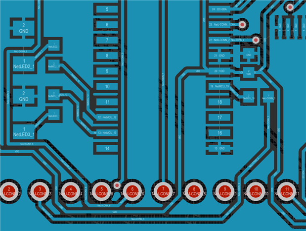
In my PCB layout, part of which is shown below, I have a copper pour serving as a ground plane. A problem that I didn't catch with this design before having it fabricated is that a couple of regions of copper pour are not actually connected to the GND net at all. Below, the pour that pads 15 and 21 are connected to, both GND pads for an MCU, is not at all connected to the GND net. Same for the region that includes the GND pad above the 1 "NetLED3_1" pad on the far right. I use the Autoroute tool to do pretty much all of the routing. Once the auto-routing is done, the polygon/copper pour gets re-poured.


So, my question is: how can I ensure that GND plane regions, which may not be contiguous with the GND plane region that is in the GND net, does get connected to the GND net with a via or something else?


I taught myself PCB layout and still have a lot to learn, so any education is welcome. Thanks!


image

  • Cancel
  • shabaz
    0 shabaz over 3 years ago

    Hi Thomas,


    You can see the faint airwaves on the screenshot that you supplied, so basically the issue was that there were airwaves that hadn't been turned into traces before you generated the CAM files. I don't use Altium so I can't point you to the specifics, but generally some things you could do would be:

    (1) run a check for airwaves if it exists, or (say) find the command to center the view onto the nearest airwave or find a way of highlighting the nearest airwave, that can be a good trick to find the very hidden airwaves.

    (2) run an error-check before generating any CAM output. There will be such a function that will provide warnings or errors, and study each warning and error to be sure if you really can ignore a warning or not.

    (3) generally when laying out a PCB, it could be worth putting a 0V via near all the microcontroller ground pins. Personally I often put the decoupling capacitor at right angles, so that one end of the decoupling capacitor goes to 0V through another via (or two). I'm not saying you should follow that, and for sure it's not suitable for all boards, but it's definitely worth checking the reference design (if it exists) to see what they do. In a similar vein, put a 0V via near any other component ground connection, unless you've got very specific reasons not to do that.

    (4) You should also check your design rules, because you've got what look like very thin copper between each pin of the microcontroller, and that's unusual. You can set the design rules so that it can't fit copper in between those pads. For the top layer, often there's no need to have the copper flood so close to the traces, you can back it off somewhat. From my perspective (others may disagree) the top flood use-case is mainly only to stop boards warping due to unbalanced amounts of copper on the two sides. This is assuming the underside of the board is being used (at least mainly) as a ground plane.

    (5) You'll get better results by manually routing. Personally I cannot do a good job routing manually in one go, so I'll do it manually in two attempts: first I'll route crudely, not taking much care about fine positioning of traces, and then I'll take a second pass, lifting up traces, to route more neatly the second time.

    I hope this info helps, good luck : )

    • Cancel
    • Vote Up 0 Vote Down
    • Cancel
  • fmilburn
    0 fmilburn over 3 years ago

    To add a little bit to the great advice from Shabaz, the airwaves that he refers to are also known as "air wires" or the "rats nest".

    • Cancel
    • Vote Up 0 Vote Down
    • Cancel
  • pizutti
    0 pizutti over 3 years ago

    So, as you are learning how to make PCB's, and sending them to manufacture, I would really suggest for you to spend a few days learning how to properly set DRC Rules, and always, always, ALWAYS, make a DRC check before sending to manufacture, this will show you any unrouted traces (that's your case), and a lot more, if you set your DRC to the manufacturer capability, you will save a lot of headache fixing issues after sending for manufacture, and possibly save you some money too, for example, if you use one single hole of 0.2mm, that's gonna cost more, trace width, etc...


    Att.

    Pablo B. Pizutti

    • Cancel
    • Vote Up 0 Vote Down
    • Cancel
  • nabelekt0
    0 nabelekt0 over 3 years ago

    Thank you for the replies! I am familiar with Design Rule Checks (DRCs), but I guess I haven't been in the habit of checking them before sending the design for manufacture. Running the DRC does indeed point out unrouted nets. I guess my question still is: Is there a way of getting the autoroute tool to try to always route every net, and if it can't give me a warning message?

    • Cancel
    • Vote Up 0 Vote Down
    • Cancel
  • shabaz
    0 shabaz over 3 years ago in reply to nabelekt0

    Hi Thomas,

    nabelekt0  wrote:

    Is there a way of getting the autoroute tool to try to always route every net, and if it can't give me a warning message?

    EAGLE (and other software) gives a percentage completion, and if it is not 100.0% then that's the (partial) indication that the autoroute is not complete, so you could look for something like that in Altium, or if there is an output report/error pane.


    I am familiar with Design Rule Checks (DRCs), but I guess I haven't been in the habit of checking them before sending the design for manufacture. Running the DRC does indeed point out unrouted nets.

    It does more than that, it points out overlaps and too-thin traces and all the other limits of physical manufacturing. By not running it, you're relying on the PCB manufacturer to correct your board where they can, and they will not/cannot do that entirely, only partially. Your board in the screenshot shows additional problem areas as mentioned before, (slivers of copper trace between integrated circuit pads) which would not have occurred if the rules were set up and checked. The problems may or may not be benign. You can imagine that slivers will peel when the board is heated, and likely cause shorts, because although your CAD program may cover it with a solder mask, in the real world machines that manufacture your PCB have size restrictions and tolerances - that's the whole point of DRC.

    On any semi-complex board (let's say more than 2-3 ICs) perhaps the chance of board success is close to 0% (this isn't an exaggeration) if you don't run the DRC, whereas if you run it and correct every error and try to follow each warning to understand what it mean, then the chance of success is very close to 100%.

    If the problem is that you forget to check for airwires and to run the DRC, you should write a checklist and mark it off each time, for each board. Checklist would be a normal way boards are done in commercial environment too, it's not trusted to memory.

    • Cancel
    • Vote Up 0 Vote Down
    • Cancel
  • nabelekt0
    0 nabelekt0 over 3 years ago in reply to shabaz

    Great tips, thanks!

    • Cancel
    • Vote Up 0 Vote Down
    • Cancel
element14 Community

element14 is the first online community specifically for engineers. Connect with your peers and get expert answers to your questions.

  • Members
  • Learn
  • Technologies
  • Challenges & Projects
  • Products
  • Store
  • About Us
  • Feedback & Support
  • FAQs
  • Terms of Use
  • Privacy Policy
  • Legal and Copyright Notices
  • Sitemap
  • Cookies

An Avnet Company © 2025 Premier Farnell Limited. All Rights Reserved.

Premier Farnell Ltd, registered in England and Wales (no 00876412), registered office: Farnell House, Forge Lane, Leeds LS12 2NE.

ICP 备案号 10220084.

Follow element14

  • X
  • Facebook
  • linkedin
  • YouTube