element14 Community
element14 Community
    Register Log In
  • Site
  • Search
  • Log In Register
  • Community Hub
    Community Hub
    • What's New on element14
    • Feedback and Support
    • Benefits of Membership
    • Personal Blogs
    • Members Area
    • Achievement Levels
  • Learn
    Learn
    • Ask an Expert
    • eBooks
    • element14 presents
    • Learning Center
    • Tech Spotlight
    • STEM Academy
    • Webinars, Training and Events
    • Learning Groups
  • Technologies
    Technologies
    • 3D Printing
    • FPGA
    • Industrial Automation
    • Internet of Things
    • Power & Energy
    • Sensors
    • Technology Groups
  • Challenges & Projects
    Challenges & Projects
    • Design Challenges
    • element14 presents Projects
    • Project14
    • Arduino Projects
    • Raspberry Pi Projects
    • Project Groups
  • Products
    Products
    • Arduino
    • Avnet Boards Community
    • Dev Tools
    • Manufacturers
    • Multicomp Pro
    • Product Groups
    • Raspberry Pi
    • RoadTests & Reviews
  • Store
    Store
    • Visit Your Store
    • Choose another store...
      • Europe
      •  Austria (German)
      •  Belgium (Dutch, French)
      •  Bulgaria (Bulgarian)
      •  Czech Republic (Czech)
      •  Denmark (Danish)
      •  Estonia (Estonian)
      •  Finland (Finnish)
      •  France (French)
      •  Germany (German)
      •  Hungary (Hungarian)
      •  Ireland
      •  Israel
      •  Italy (Italian)
      •  Latvia (Latvian)
      •  
      •  Lithuania (Lithuanian)
      •  Netherlands (Dutch)
      •  Norway (Norwegian)
      •  Poland (Polish)
      •  Portugal (Portuguese)
      •  Romania (Romanian)
      •  Russia (Russian)
      •  Slovakia (Slovak)
      •  Slovenia (Slovenian)
      •  Spain (Spanish)
      •  Sweden (Swedish)
      •  Switzerland(German, French)
      •  Turkey (Turkish)
      •  United Kingdom
      • Asia Pacific
      •  Australia
      •  China
      •  Hong Kong
      •  India
      •  Korea (Korean)
      •  Malaysia
      •  New Zealand
      •  Philippines
      •  Singapore
      •  Taiwan
      •  Thailand (Thai)
      • Americas
      •  Brazil (Portuguese)
      •  Canada
      •  Mexico (Spanish)
      •  United States
      Can't find the country/region you're looking for? Visit our export site or find a local distributor.
  • Translate
  • Profile
  • Settings
Altium CircuitStudio
  • Products
  • Manufacturers
  • Altium CircuitStudio
  • More
  • Cancel
Altium CircuitStudio
Altium CircuitStudio Forum my smd component things its a thru hole
  • Blog
  • Forum
  • Documents
  • Events
  • Polls
  • Members
  • Mentions
  • Sub-Groups
  • Tags
  • More
  • Cancel
  • New
Join Altium CircuitStudio to participate - click to join for free!
Actions
  • Share
  • More
  • Cancel
Forum Thread Details
  • Locked Locked
  • Replies 5 replies
  • Subscribers 85 subscribers
  • Views 664 views
  • Users 0 members are here
Related
This discussion has been locked.
You can no longer post new replies to this discussion. If you have a question you can start a new discussion

my smd component things its a thru hole

ulao
ulao over 1 year ago

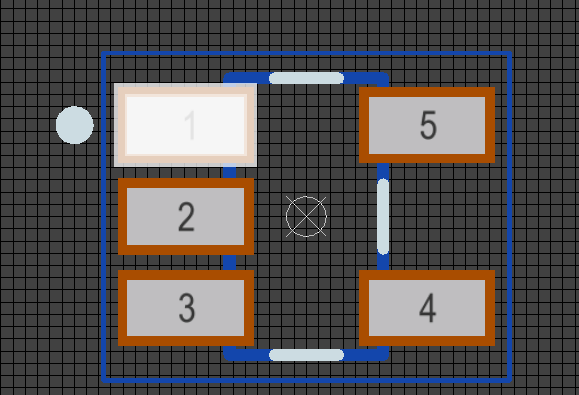
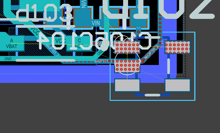
The below info is a test just to prove my issue, but in short the SMD thinks its a thru hole on the PCB.

Here I put it on the edge where there are no conflicts on the layer I put it on
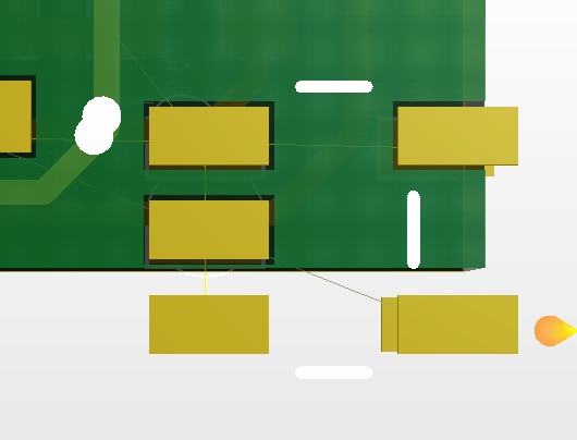
image

here is the 3d view

...

I had to make my own sch library files but the foot print was available. I made my own sch and then added the foot print. But when adding to my PCB it conflicts on the under side layer. It looks likes pads are drawn on both side.

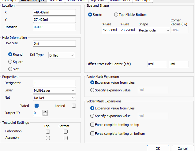
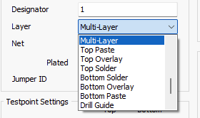
I see no way to draw pads on both layer in the editor how was that done?

image

  • Cancel
  • ulao
    ulao over 1 year ago

    looks like the 3d image broke this was the image

    image

    I also see thisimage

    can I just tell it top layer instead of multi ?

    • Cancel
    • Vote Up 0 Vote Down
    • Cancel
  • dougw
    dougw over 1 year ago in reply to ulao

    It sounds like you need to edit the footprint to remove the pads from the bottom layer.

    If the properties window you showed is global properties, you probably still want multilayer.

    • Cancel
    • Vote Up 0 Vote Down
    • Cancel
  • ulao
    ulao over 1 year ago in reply to dougw

    that was a property for a pad in the footprint. How do I do this for the entire footprint, or do I need to do each pad? So I just change to top solder?

    image

    • Cancel
    • Vote Up 0 Vote Down
    • Cancel
  • dougw
    dougw over 1 year ago in reply to ulao

    I don't know this CAD tool - my CAD software allows operating on a group at the same time.

    • Cancel
    • Vote Up 0 Vote Down
    • Cancel
  • GabeFromSpace
    GabeFromSpace over 1 year ago in reply to ulao

    You are correct. You can just set it to the top layer instead of multi. Top layer will also automatically include other layers such as the solder mask and paste mask.

    • Cancel
    • Vote Up 0 Vote Down
    • Cancel
element14 Community

element14 is the first online community specifically for engineers. Connect with your peers and get expert answers to your questions.

  • Members
  • Learn
  • Technologies
  • Challenges & Projects
  • Products
  • Store
  • About Us
  • Feedback & Support
  • FAQs
  • Terms of Use
  • Privacy Policy
  • Legal and Copyright Notices
  • Sitemap
  • Cookies

An Avnet Company © 2025 Premier Farnell Limited. All Rights Reserved.

Premier Farnell Ltd, registered in England and Wales (no 00876412), registered office: Farnell House, Forge Lane, Leeds LS12 2NE.

ICP 备案号 10220084.

Follow element14

  • X
  • Facebook
  • linkedin
  • YouTube