I had questions about splitting a power or ground, etc. plane on an internal layer - which are more or less answered here:
How to Assign Net Name to Internal Layer
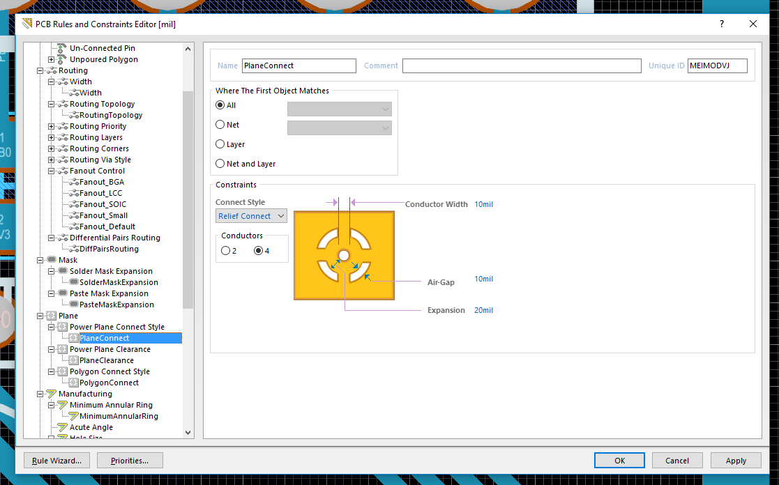
That finished, there seems to be no way to edit the polygon pour options on these internal layers - so you're stuck with whatever clearances, cutouts, and tab connections to vias that are hard coded in CS? what?
here's a screen shot of the feature I want to edit:
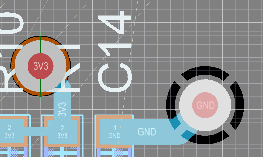
you can see that this is the GND internal plane that is highlighted in gray. You can also see a power plane 3.3V via to the left. The GND via clearance and connection - the perimeter is kinda huge, and the connection is thin. maybe I want to edit that.
More worrisome is the 3.3V via clearance. looks small - although i see how the via diameter isn't the same in the internal layers. That being said, some of the boards that I design, have HV on the internal layers, where clearance needs to be under My control. how can we edit these internal layer polygon pours? its important!