element14 Community
element14 Community
    Register Log In
  • Site
  • Search
  • Log In Register
  • Community Hub
    Community Hub
    • What's New on element14
    • Feedback and Support
    • Benefits of Membership
    • Personal Blogs
    • Members Area
    • Achievement Levels
  • Learn
    Learn
    • Ask an Expert
    • eBooks
    • element14 presents
    • Learning Center
    • Tech Spotlight
    • STEM Academy
    • Webinars, Training and Events
    • Learning Groups
  • Technologies
    Technologies
    • 3D Printing
    • FPGA
    • Industrial Automation
    • Internet of Things
    • Power & Energy
    • Sensors
    • Technology Groups
  • Challenges & Projects
    Challenges & Projects
    • Design Challenges
    • element14 presents Projects
    • Project14
    • Arduino Projects
    • Raspberry Pi Projects
    • Project Groups
  • Products
    Products
    • Arduino
    • Avnet & Tria Boards Community
    • Dev Tools
    • Manufacturers
    • Multicomp Pro
    • Product Groups
    • Raspberry Pi
    • RoadTests & Reviews
  • About Us
  • Store
    Store
    • Visit Your Store
    • Choose another store...
      • Europe
      •  Austria (German)
      •  Belgium (Dutch, French)
      •  Bulgaria (Bulgarian)
      •  Czech Republic (Czech)
      •  Denmark (Danish)
      •  Estonia (Estonian)
      •  Finland (Finnish)
      •  France (French)
      •  Germany (German)
      •  Hungary (Hungarian)
      •  Ireland
      •  Israel
      •  Italy (Italian)
      •  Latvia (Latvian)
      •  
      •  Lithuania (Lithuanian)
      •  Netherlands (Dutch)
      •  Norway (Norwegian)
      •  Poland (Polish)
      •  Portugal (Portuguese)
      •  Romania (Romanian)
      •  Russia (Russian)
      •  Slovakia (Slovak)
      •  Slovenia (Slovenian)
      •  Spain (Spanish)
      •  Sweden (Swedish)
      •  Switzerland(German, French)
      •  Turkey (Turkish)
      •  United Kingdom
      • Asia Pacific
      •  Australia
      •  China
      •  Hong Kong
      •  India
      • Japan
      •  Korea (Korean)
      •  Malaysia
      •  New Zealand
      •  Philippines
      •  Singapore
      •  Taiwan
      •  Thailand (Thai)
      • Vietnam
      • Americas
      •  Brazil (Portuguese)
      •  Canada
      •  Mexico (Spanish)
      •  United States
      Can't find the country/region you're looking for? Visit our export site or find a local distributor.
  • Translate
  • Profile
  • Settings
Altium CircuitStudio
  • Products
  • Manufacturers
  • Altium CircuitStudio
  • More
  • Cancel
Altium CircuitStudio
Altium CircuitStudio Forum Reconciling layers between the old Mech12 and new Assembly Top
  • Blog
  • Forum
  • Documents
  • Events
  • Polls
  • Members
  • Mentions
  • Sub-Groups
  • Tags
  • More
  • Cancel
  • New
Join Altium CircuitStudio to participate - click to join for free!
Actions
  • Share
  • More
  • Cancel
Forum Thread Details
  • Locked Locked
  • Replies 4 replies
  • Subscribers 89 subscribers
  • Views 579 views
  • Users 0 members are here
Related
This discussion has been locked.
You can no longer post new replies to this discussion. If you have a question you can start a new discussion

Reconciling layers between the old Mech12 and new Assembly Top

jmarkwolf
jmarkwolf over 7 years ago

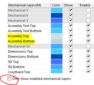
I used Mech12 & Mech13 as my top and bottom assembly drawing layers in Altium for many years. All my footprint libraries have "data" on these layers.


Now that I've switched to Circuit Studio anything on Mech12 in the PCB library editor comes in on the "Dimensions Bottom" layer in the CS PCB editor. I think I want it on the CS "Assembly Top" layer. There is no Mech12 in the layers list in the CS PCB editor, nor is there a "Assembly Top" layer in the CS PCB library editor.


So how can I get this Mech12 library data on the PCB "Assembly Top" layer?

  • Cancel

Top Replies

  • e14softwareuk
    e14softwareuk over 7 years ago +1
    My guess on this one is you would need to edit your library components to move the data to the new layers. I believe Mech12 = Dimensions Bottom and Mech13 = 3D Top. There are Assembly Top and Assembly…
  • e14softwareuk
    e14softwareuk over 7 years ago

    My guess on this one is you would need to edit your library components to move the data to the new layers. I believe Mech12 = Dimensions Bottom and Mech13 = 3D Top. There are Assembly Top and Assembly Bottom within CS.

    image

    • Cancel
    • Vote Up +1 Vote Down
    • Cancel
  • jmarkwolf
    jmarkwolf over 7 years ago in reply to e14softwareuk

    Thank you Peter. That's the ticket.


    The layers actually map from the old to the new sequentially, not by name, so all I had to do was change everything on my Mech12 to Mech8 then update the PCB with a right click on the library item in question. It magically showed up on the Dimensions Top layer in the new PCB. I thought it was going to be more diabolical than that!

    • Cancel
    • Vote Up 0 Vote Down
    • Cancel
  • optoeng
    optoeng over 7 years ago in reply to e14softwareuk

    This thread seems to contain an interesting clue to a serious problem we have had since converting to CS months ago: Layer names seem to be editable, but at various times you find out that they really are not editable. Instead, there is some kind of list of 'absolute' layer names that manifests itself at times as in the original post here. For us, the biggest problem with that is that ODB++ output files and folders have names with UPPERCASE characters. This is expressly forbidden in the ODB++ Standard, and the file structure regularly crashes ODB++ viewers. We have to manually edit all names with uppercase characters before submitting ODB++ files to our contract manufacturers, and this is a tedious process. The reason for my replying to this thread, is that I see that Peter Barnard has actually replied to the message here, and I am desperately hoping for an actual reply myself. To date, no one from CS support has ever contacted me about this issue.

    • Cancel
    • Vote Up 0 Vote Down
    • Cancel
  • e14softwareuk
    e14softwareuk over 7 years ago in reply to optoeng

    Each layer has more than one name and only one of the names is editable. Renaming layers can cause problems, for example assembly plots. My guess is that the 'uneditable' names are used for matching in some circumstances and confusion occurs because you can view the edited names and think the layer name has changed. It is true that the ODB++ output is an issue and is something Altium are aware of but as yet a fix has not been issued.

    • Cancel
    • Vote Up 0 Vote Down
    • Cancel
element14 Community

element14 is the first online community specifically for engineers. Connect with your peers and get expert answers to your questions.

  • Members
  • Learn
  • Technologies
  • Challenges & Projects
  • Products
  • Store
  • About Us
  • Feedback & Support
  • FAQs
  • Terms of Use
  • Privacy Policy
  • Legal and Copyright Notices
  • Sitemap
  • Cookies

An Avnet Company © 2026 Premier Farnell Limited. All Rights Reserved.

Premier Farnell Ltd, registered in England and Wales (no 00876412), registered office: Farnell House, Forge Lane, Leeds LS12 2NE.

ICP 备案号 10220084.

Follow element14

  • X
  • Facebook
  • linkedin
  • YouTube