element14 Community
element14 Community
    Register Log In
  • Site
  • Search
  • Log In Register
  • About Us
  • Community Hub
    Community Hub
    • What's New on element14
    • Feedback and Support
    • Benefits of Membership
    • Personal Blogs
    • Members Area
    • Achievement Levels
  • Learn
    Learn
    • Ask an Expert
    • eBooks
    • element14 presents
    • Learning Center
    • Tech Spotlight
    • STEM Academy
    • Webinars, Training and Events
    • Learning Groups
  • Technologies
    Technologies
    • 3D Printing
    • FPGA
    • Industrial Automation
    • Internet of Things
    • Power & Energy
    • Sensors
    • Technology Groups
  • Challenges & Projects
    Challenges & Projects
    • Design Challenges
    • element14 presents Projects
    • Project14
    • Arduino Projects
    • Raspberry Pi Projects
    • Project Groups
  • Products
    Products
    • Arduino
    • Avnet Boards Community
    • Dev Tools
    • Manufacturers
    • Multicomp Pro
    • Product Groups
    • Raspberry Pi
    • RoadTests & Reviews
  • Store
    Store
    • Visit Your Store
    • Choose another store...
      • Europe
      •  Austria (German)
      •  Belgium (Dutch, French)
      •  Bulgaria (Bulgarian)
      •  Czech Republic (Czech)
      •  Denmark (Danish)
      •  Estonia (Estonian)
      •  Finland (Finnish)
      •  France (French)
      •  Germany (German)
      •  Hungary (Hungarian)
      •  Ireland
      •  Israel
      •  Italy (Italian)
      •  Latvia (Latvian)
      •  
      •  Lithuania (Lithuanian)
      •  Netherlands (Dutch)
      •  Norway (Norwegian)
      •  Poland (Polish)
      •  Portugal (Portuguese)
      •  Romania (Romanian)
      •  Russia (Russian)
      •  Slovakia (Slovak)
      •  Slovenia (Slovenian)
      •  Spain (Spanish)
      •  Sweden (Swedish)
      •  Switzerland(German, French)
      •  Turkey (Turkish)
      •  United Kingdom
      • Asia Pacific
      •  Australia
      •  China
      •  Hong Kong
      •  India
      •  Korea (Korean)
      •  Malaysia
      •  New Zealand
      •  Philippines
      •  Singapore
      •  Taiwan
      •  Thailand (Thai)
      • Americas
      •  Brazil (Portuguese)
      •  Canada
      •  Mexico (Spanish)
      •  United States
      Can't find the country/region you're looking for? Visit our export site or find a local distributor.
  • Translate
  • Profile
  • Settings
Altium CircuitStudio
  • Products
  • Manufacturers
  • Altium CircuitStudio
  • More
  • Cancel
Altium CircuitStudio
Altium CircuitStudio Forum Component has been flipped and mirrored on same layer - why and how to detect
  • Blog
  • Forum
  • Documents
  • Events
  • Polls
  • Members
  • Mentions
  • Sub-Groups
  • Tags
  • More
  • Cancel
  • New
Join Altium CircuitStudio to participate - click to join for free!
Actions
  • Share
  • More
  • Cancel
Forum Thread Details
  • Locked Locked
  • Replies 6 replies
  • Subscribers 89 subscribers
  • Views 4696 views
  • Users 0 members are here
  • troubleshooting
  • footprint
  • component vault
  • circuitstudio
Related
This discussion has been locked.
You can no longer post new replies to this discussion. If you have a question you can start a new discussion

Component has been flipped and mirrored on same layer - why and how to detect

jaza_tom
jaza_tom over 7 years ago

I have encountered a very strange problem.


At first I thought it was  a bug that makes Altium Vault components inconsistent in terms of their footprint when placing multiple instances of that component.


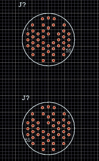
See video below to see what I mean.  D2_1 and D2_2 are the same component, but their footprints appear to be mirror images of one another.


You don't have permission to edit metadata of this video.
Edit media
x
image
Upload Preview
image


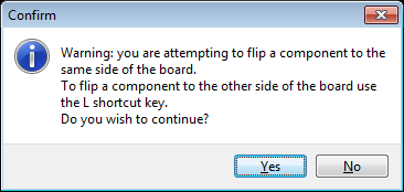
Upon further friggin around I was able to replicate this phenomenon by copying the component, and then pressing the X button when placing it.


See below video for what I mean:


You don't have permission to edit metadata of this video.
Edit media
x
image
Upload Preview
image


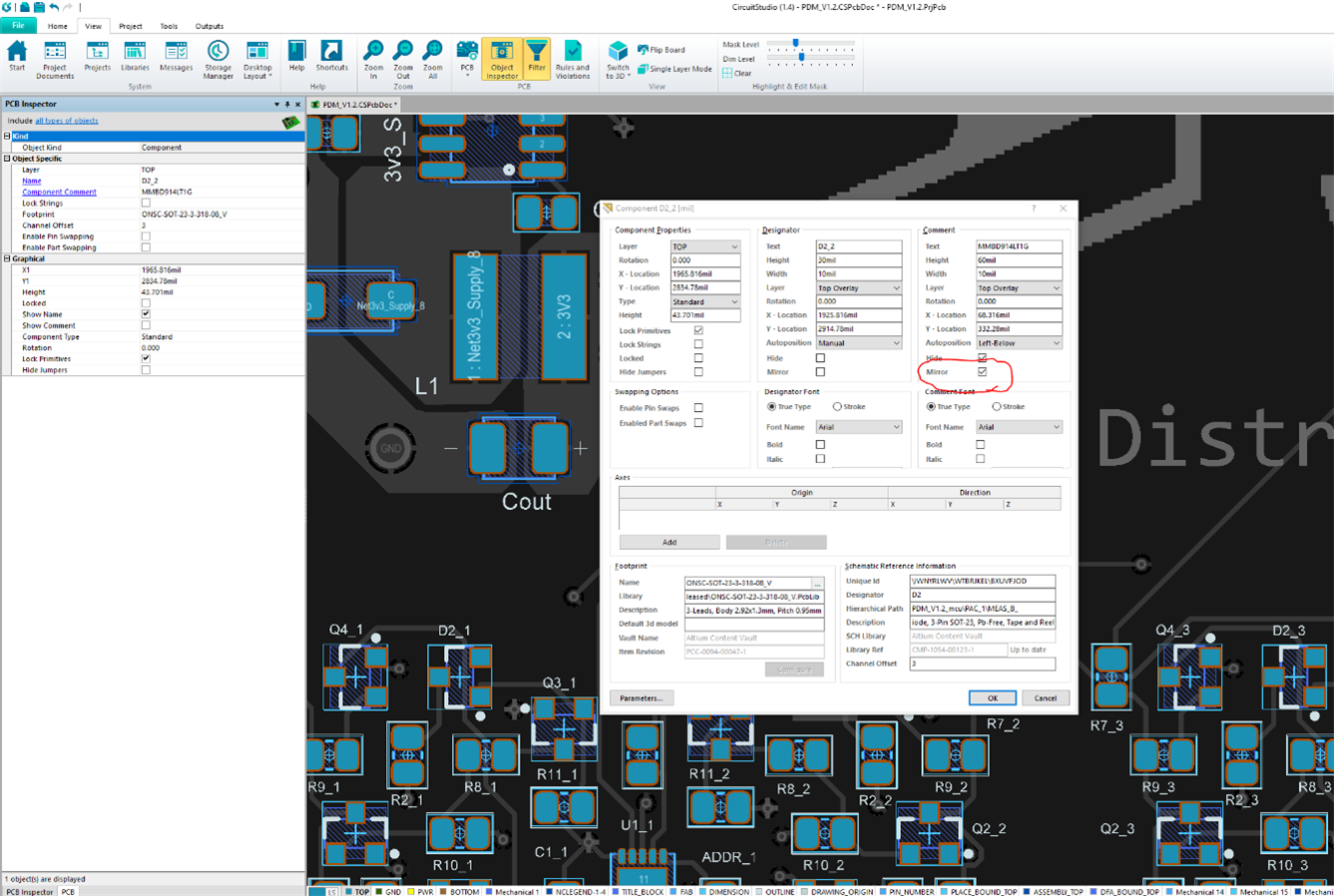
After yet more friggin around, I was able to determine that the erroneous footprint was indeed likely caused by inadvertently pressing the X button during placement of the component by double-clicking on the component and taking a peek at it's Comment's Mirror property.


image


A couple of things:


  1. How can I figure out which components on my board have had their footprints mirrored using the X and Y placement modifiers?  I see no property that specifies whether the component itself has been mirrored (though there does appear to be an accessible mirror property for the designator and comment).
  2. Why is there an option to mirror a component's footprint in the first place?  I can't think of any use cases for such a feature, and if you don't realize it is happening when it occurs, you are effectively now using an erroneous footprint.


In my case, this error got copied 6 times, meaning that each on of my prototype boards have multiple problems and are now built and faulty.


Not impressed!

  • Cancel

Top Replies

  • e14softwareuk
    e14softwareuk over 7 years ago in reply to jaza_tom +1
    I've logged an improvement suggestion with Altium to remove the X,Y flip for the PCB editor.
  • e14softwareuk
    e14softwareuk over 7 years ago

    Sorry to hear about the board problems and thanks for the video. In the video you show the warning dialog when attempting to use the X or Y command

    image

    Are you saying that at some point you could use X and Y without this warning appearing?


    I'm not sure of any automated way to detect such components once mirrored.

    • Cancel
    • Vote Up 0 Vote Down
    • Cancel
  • jaza_tom
    jaza_tom over 7 years ago in reply to e14softwareuk

    I'm not sure if the warning appeared or not, it would have been over a week ago since it happened.


    If the warning did appear, it would have been while copying/placing a whole group of components as part of a multi-channel layout where I wanted to mirror the relative position of all components with respect to one another (not change the footprint of each component).


    Can you (or anyone reading this) think of a scenario in which you would want to dynamically change the pin assignments of a component's footprint by pressing "X" or "Y" while placing the component?


    This "feature" seems ill-conceived.  Footprint physical pin locations should not be changeable during placement.  In my experimentation on this "feature", seems that if you flip the footprint of a component, and then make a change to that footprint in it's parent library and propagate it to the PCB, it flips the footprint back to its original (correct) orientation.  So, even if for some reason this "feature" was useful to someone somewhere, it will break down the second they attempt to propagate parent PCB library changes to the board they are editing.


    Not sure if you are the person to bring this to, but unless there is a documented useful use case for this "feature", I think it should be removed in the next released update to CircuitStudio (which is when, by the way?).

    • Cancel
    • Vote Up 0 Vote Down
    • Cancel
  • e14softwareuk
    e14softwareuk over 7 years ago in reply to jaza_tom

    I've logged an improvement suggestion with Altium to remove the X,Y flip for the PCB editor.

    • Cancel
    • Vote Up +1 Vote Down
    • Cancel
  • herrcespedes
    herrcespedes over 7 years ago in reply to e14softwareuk

    I would vote against removing the feature. it is useful for example using asymmetrical connectors. I created a footprint for a mil s
    spec connector, where to introduce male and female, I had to mirror the footprint. If the option wasn't available, I would have had to create two footprints. manually introducing all these pads with xy coordinates is very tedious... and mirroring saves a lot of time.  as long as a clear warning appears at the time of mirroring, I see no issue, with allowing this feature. perhaps removing the hotkey would aid in preventing accidental flipping, but it should be an option available through the inspector at least.
    image

    • Cancel
    • Vote Up 0 Vote Down
    • Cancel
  • e14softwareuk
    e14softwareuk over 7 years ago in reply to herrcespedes

    Hi Ricardo many thanks for the use case for mirroring. Although a suggestion was logged with Altium for removal it did not look likely to happen because of the big warning message that is given if you try to use this feature. Sounds like the current situation is the best compromise - the feature works but generates a warning when used.

    • Cancel
    • Vote Up 0 Vote Down
    • Cancel
  • lamabrew
    lamabrew over 7 years ago in reply to e14softwareuk

    One other component where this is maybe helpful (I say may be as pin swapping pairs is probably the correct way) is common mode chokes, which have a land pattern that can be swapped either way.

    image

    While I use this type of part I don't think I've had need to resort to flipping the footprint to improve routing as I try and make sure the schematics consider the layout. But it could be useful to flip in some cases?

    • Cancel
    • Vote Up 0 Vote Down
    • Cancel
element14 Community

element14 is the first online community specifically for engineers. Connect with your peers and get expert answers to your questions.

  • Members
  • Learn
  • Technologies
  • Challenges & Projects
  • Products
  • Store
  • About Us
  • Feedback & Support
  • FAQs
  • Terms of Use
  • Privacy Policy
  • Legal and Copyright Notices
  • Sitemap
  • Cookies

An Avnet Company © 2025 Premier Farnell Limited. All Rights Reserved.

Premier Farnell Ltd, registered in England and Wales (no 00876412), registered office: Farnell House, Forge Lane, Leeds LS12 2NE.

ICP 备案号 10220084.

Follow element14

  • X
  • Facebook
  • linkedin
  • YouTube