element14 Community
element14 Community
    Register Log In
  • Site
  • Search
  • Log In Register
  • Community Hub
    Community Hub
    • What's New on element14
    • Feedback and Support
    • Benefits of Membership
    • Personal Blogs
    • Members Area
    • Achievement Levels
  • Learn
    Learn
    • Ask an Expert
    • eBooks
    • element14 presents
    • Learning Center
    • Tech Spotlight
    • STEM Academy
    • Webinars, Training and Events
    • Learning Groups
  • Technologies
    Technologies
    • 3D Printing
    • FPGA
    • Industrial Automation
    • Internet of Things
    • Power & Energy
    • Sensors
    • Technology Groups
  • Challenges & Projects
    Challenges & Projects
    • Design Challenges
    • element14 presents Projects
    • Project14
    • Arduino Projects
    • Raspberry Pi Projects
    • Project Groups
  • Products
    Products
    • Arduino
    • Avnet Boards Community
    • Dev Tools
    • Manufacturers
    • Multicomp Pro
    • Product Groups
    • Raspberry Pi
    • RoadTests & Reviews
  • Store
    Store
    • Visit Your Store
    • Choose another store...
      • Europe
      •  Austria (German)
      •  Belgium (Dutch, French)
      •  Bulgaria (Bulgarian)
      •  Czech Republic (Czech)
      •  Denmark (Danish)
      •  Estonia (Estonian)
      •  Finland (Finnish)
      •  France (French)
      •  Germany (German)
      •  Hungary (Hungarian)
      •  Ireland
      •  Israel
      •  Italy (Italian)
      •  Latvia (Latvian)
      •  
      •  Lithuania (Lithuanian)
      •  Netherlands (Dutch)
      •  Norway (Norwegian)
      •  Poland (Polish)
      •  Portugal (Portuguese)
      •  Romania (Romanian)
      •  Russia (Russian)
      •  Slovakia (Slovak)
      •  Slovenia (Slovenian)
      •  Spain (Spanish)
      •  Sweden (Swedish)
      •  Switzerland(German, French)
      •  Turkey (Turkish)
      •  United Kingdom
      • Asia Pacific
      •  Australia
      •  China
      •  Hong Kong
      •  India
      •  Korea (Korean)
      •  Malaysia
      •  New Zealand
      •  Philippines
      •  Singapore
      •  Taiwan
      •  Thailand (Thai)
      • Americas
      •  Brazil (Portuguese)
      •  Canada
      •  Mexico (Spanish)
      •  United States
      Can't find the country/region you're looking for? Visit our export site or find a local distributor.
  • Translate
  • Profile
  • Settings
Altium CircuitStudio
  • Products
  • Manufacturers
  • Altium CircuitStudio
  • More
  • Cancel
Altium CircuitStudio
Altium CircuitStudio Forum Creating through hole in pcb library footprint
  • Blog
  • Forum
  • Documents
  • Events
  • Polls
  • Members
  • Mentions
  • Sub-Groups
  • Tags
  • More
  • Cancel
  • New
Join Altium CircuitStudio to participate - click to join for free!
Actions
  • Share
  • More
  • Cancel
Forum Thread Details
  • Locked Locked
  • Replies 1 reply
  • Subscribers 86 subscribers
  • Views 1086 views
  • Users 0 members are here
  • circuit studio
Related
This discussion has been locked.
You can no longer post new replies to this discussion. If you have a question you can start a new discussion

Creating through hole in pcb library footprint

doov123
doov123 over 6 years ago

I'm evaluating circuit studio and trying to make a footprint for this switch: LS12-Side-press type-Tactile switch | CITIZEN ELECTRONICS CO.,LTD.


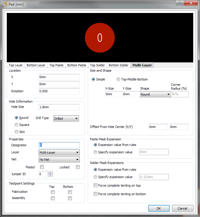
As seen the land pattern requires two mechanical through holes that are not electrically connected anything.  What's the best way to add a hole to a footprint in circuit studio?  I've tried using the polygon pour cutout with the board cutout option selected, but I can't figure out how to do a round hole and when I view the footprint in 3D it doesn't appear to render as a hole at all.


Additionally what's the best way to create the custom/non rectangular pads seen in the datasheet?  Is it better to try to create an oversized pad and cut away or to create a smaller sized pad and add material using arcs etc?

  • Cancel
  • lamabrew
    lamabrew over 6 years ago

    For the hole just add a pad that's not plated and no copper, for example:

    image


    which is from a power connector I made:

    image


    (I can't comment on odd pad shapes as I haven't had to do that yet.)

    • Cancel
    • Vote Up 0 Vote Down
    • Cancel
element14 Community

element14 is the first online community specifically for engineers. Connect with your peers and get expert answers to your questions.

  • Members
  • Learn
  • Technologies
  • Challenges & Projects
  • Products
  • Store
  • About Us
  • Feedback & Support
  • FAQs
  • Terms of Use
  • Privacy Policy
  • Legal and Copyright Notices
  • Sitemap
  • Cookies

An Avnet Company © 2025 Premier Farnell Limited. All Rights Reserved.

Premier Farnell Ltd, registered in England and Wales (no 00876412), registered office: Farnell House, Forge Lane, Leeds LS12 2NE.

ICP 备案号 10220084.

Follow element14

  • X
  • Facebook
  • linkedin
  • YouTube