
Protection of USB 2.0 Applications
The Protection of USB 2.0 Applications
ANP002C BY JOCHEN BAIER
1. ESD-confirm USB Interfaces
The USB-Interface might be the most distributed PC interface in the world. The usage in industry applications is more and more common. Let’s have a closer look to the special environmental conditions of industry applications.
That there are real concerns regarding the robustness against EMI and ESD is written in Intel’s “High Speed USB Platform Design Guidelines”. Intel recommends the usage of a common mode choke for EMI suppressions and another component for protection against ESD pulses.
Würth Elektronik offers all these types of products.
- The WE-CNSW common mode choke was developed for EMI suppression on high speed signal lines
- For ESD suppression the TVS diode arrays WE-TVS with very low capacitances (<2pF) or the ESD Suppressors WE-VE (capacitances down to 0.05pF) are your preferred choice.
But for outstanding EMI behaviour it is absolutely necessary to protect the power supply (Vbus) as well. A lot of design engineers forget this important point and wonder themselves when their product don’t pass all the tests in an EMI lab.
Two typical schematics for optimized protection of one or two USB ports are shown below:
With one TVS diode array WE-TVS you can fully protect two USB lines. All four signal lines as well as the common power supply are well protected.
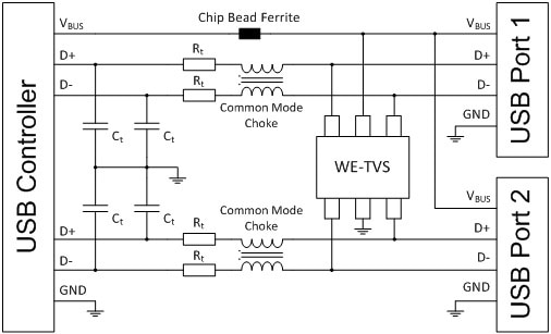
Figure 1: Two-Port-USB-Interface with ESD-Protection
For further optimization, i.e. to filter incoming common mode noise as well as differential mode noise from USB line, a LC filter is built with the common mode choke WE-CNSW and the capacitors. For power supply lines very good noise suppressions can be eached with a chip bead ferrite, like the Würth Elektronik WE-CBF series.
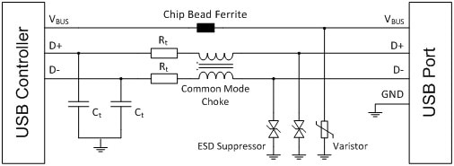
Figure 2: In contrast to the shielding of the dataline no low capacitive ESD suppressor is necessary at the power supply
Single line protection components like ESD suppressors series WE-VE also have to be connected from signal line to GND. For power line protection it is not necessary to use a low cap ESD suppressor, you might prefer a standard SMD varistor which can withstand higher surges and higher transient energies.
2. About TVS Diodes
Würth Elektronik launched the TVS diodes array series called WE-TVS. These TVS diodes arrays include three main functions:
- protection against ESD pulses according to EN 61000-4-2
- protection against surge pulses according to EN 61000-4-5
- protection against EFT pulses according to EN 61000-4-4
WE-TVS series are high performance designed TVS diode arrays which include surge rated diodes. They are the best choice to protect high speed data lines like USB 2.0, DVI or LAN from over-voltages. The WE-TVS series exceeds the requirements outlined in EN 61000-4-2. Due to their ultra low capacitance (<2.0 pF) they are nearly invisible on the signal lines.
3. About ESD Suppressors
The ESD suppressors are special raised varistors with a low and defined intrinsic capacitance. Würth Elektronik has three different series:
- WE-VE standard series: Capacitances of 1pF to 120pF and voltages from 5V to 24V
- WE-VE “ULC” series: Capacitance of 0.2pF, suitable for signal lines up to 12V
- WE-VE femtoF series: Capacitance of 0.05pF and rated voltages of 6V, 14V and 26V
3.1. Why ESD Protection?
Since the first electronic developments, all the parts are subjected to electrostatic discharge. ESD events have peak voltages up to 30kV and therewith they are very dangerous for all kind of integrated circuits.
However, some state-of-the-art ICs are protected against ESD pulses but real world conditions show daily that an additional protection device is indispensable. On the one hand to have the whole board ESD free and on the other hand to develop more reliable products to satisfy the needs of your customers.
3.2. Why EMI Suppression?
With the increase in electronic/electrical products and the need to have wireless connectivity in today’s global markets, there is an increased requirement to ensure that your product is immune to the impacts caused by both the intentional and un-intentional RF environment. Only if you consider now which EMI phenomena impacts on the product, will you be able to design in the appropriate protection and reduce time to market.
In addition, the product must not generate excessive levels of EMI and this is typically assessed by an EMC Test Laboratory, and should the product fail then costs to implement remedial work will increase aggressively.
4. Different Protection Devices for Different Requirements
There are four different TVS diode arrays and five different ESD Suppressors available:
WE Order Code | Package | Pin Conf. | I/O / VDD Lines | VRWM | CIN | IPP | VESD | VCl ESD | VDD can float | Farnell Order Code |
SOT23-5L | 1 | 2/1 | 5V | 2.0 pF | 12 A | 20 kV | 13 V | NO | 1748616 | |
SOT23-6L | 2 | 4/1 | 5V | 2.0 pF | 12 A | 20 kV | 13 V | NO | 1748615 | |
SOT23-6L | 2 | 4/1 | 5V | 1.0pF | 5A | 15kV | 14V | NO | 1748613 | |
SOT23-6L | 3 | 4/1 | 5V | 0.5 pF | 4A | 16kV | 12V | YES | 1748614 | |
0402 | 4 | 1 | 5V | 0.2 pF | - | 8kV | 17V | - | 1850151 | |
0603 | 4 | 1 | 5V | 0.2 pF | - | 8kV | 30V | - | 1850152 |
 |  |  | Pin Configuration 4
|
| Pin Configuration 1 | Pin Configuration 2 | Pin Configuration 3 | Pin Configuration 5 |

Figure 3: Several Pin-Configurations of WE-TVS series
4.1. How to find the Suitable Part?
- You have supply voltage to connect for rail-to-rail clamping
--> take TVS diode
- You don’t have supply voltage or do prefer ceramic components
--> take TVS diode where VDD pin can float or take WE-VE ESD suppressor
- Which maximum capacitance can you add to your data lines to pass the eye pattern test?
--> for USB 2.0 line capacitances up to 5pF shouldn’t cause any trouble
- What’s the maximum expected ESD voltage that can occur?
- Do you want to protect one or two USB lines? However, connecting one USB data line with two I/O
ports of TVS diode lets you get a better performance --> select array type
Answer all these questions and you will find the most suitable part for you. We recommend for one USB 2.0 port 824011824011 and for two USB 2.0 ports 824015824015. Designers preferring single line components may choose p/n 8230705002982307050029 or 8230605002982306050029.
5. Eye Pattern Test
After making a choice of protection element you have to ensure that your whole interface design meets the requirements of USB specification. Therefore you can use our protection devices with a small capacitance which is nearly invisible on the signal lines.
| Port 1: D+ | Port 1: D- | Port 2: D+ | Port 2: DEye |
 | |||
Figure 4: Eye pattern test without any protection component placed on two USB 2.0 differential signal lines.
| Port 1: D+ | Port 1: D- | Port 2: D+ | Port 2: DEye |
 | |||
Figure 5: Eye pattern test with TVS diode WE-TVS 824015
The eye pattern test shows that the WE-TVS do not disturb the USB 2.0 signal. You get the same results with our other listed TVS diodes and with the ESD suppressors as well. The following table shows the cutting edge ultra low capacitance technology of Würth Elektronik. This technology enables a channel to channel capacitance which is almost invisible at normal operating conditions.
Order Code | Order Code Package | I/O | VRWM | CIN | CX |
824015824015 | SOT23-6L | 4 | 5 | 2pF | 0,1pF |
Competitor S | SOT23-6L | 4 | 5 | 3pF | 1,5pF |
824001824001 | SOT23-6L | 4 | 5 | 1pF | 0,1pF |
Competitor P | SOT23-6L | 4 | 5 | 3pF | 1,5pF |
I/O | Number of I/O lines the TVS-Diode can protect | ||||
VRWM | Max. reverse working voltage | ||||
CIN | Input capacitance at I/O pin via. GND (VIN = 2,5V, VDD=5V) | ||||
CX | Input capacitance between I/O pins (VIN = 2,5V, VDD=5V) | ||||
Table 1: Comparison of Parts for Capacitance
6. Testing the Protection Level of ESD Protection Devices
The easiest way to measure the protection level is to apply an ESD pulse to your electronic circuit with the ESD protection device and measure the peak voltage of this ESD pulse before and after the protection device. But this way carries out different problems.
Due to high frequency and wide range of ESD pulse (few MHz to some GHZ) high frequency refractions will occur during the measurement. The absolute peak voltage and the spike voltages during the refractions are an indicator for better and worse protection, but you cannot indicate the definitive clamping voltage. And by the way, this is not a reliable and repeatable measurement!
Engineers being familiar with semiconductor products do know the TLP measuring method. The TLP (transmission line pulsing) method is an accurate measurement system which allows - due to all measurements are done in a 50Ω-System - repeatable and very accurate measurements.
A defined current impulse (left) is charged into the protection component and the resulting voltage across it is measured (middle). This procedure is repeated with increasing TLP currents. As a result you get the TLP curve (right).
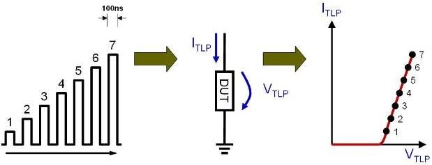
Figure 6: TLP measurement system with corresponding TLP curve
This measurement can be done for VDD and I/O pins. The lower the voltage you measure, the better is the protection device and therewith the reliability of your electronic circuit. Thanks to the built in snap-back technology, Würth Elektronik TVS diodes have the lowest ESD clamping voltage on the market. This you can see with a short view at the TLP curves.
Order Code | Package | I/O | VRWM | VCl,IO | VCl,VDD | VESD | CIN | IPP |
SOT23-6L | 4 | 5 | 12 | 7,5 | 12kV | 2pF | 12A | |
Competitor S | SOT23-6L | 4 | 5 | 22 | 15,5 | 15kV | 3pF | 12A |
SOT23-6L | 4 | 5 | 14 | 9 | 8kV | 1pF | 5A | |
Competitor P | SOT23-6L | 4 | 5 | 28 | 19 | 8kV | 3pF | 6A |
I/O | Number of I/O lines the TVS-Diode can protect | |||||||
VRWM | Max. reverse working voltage | |||||||
VCl,IO | ESD clamping voltage at I/O pin (IEC 61000-4-2, contact mode at 6kV) | |||||||
VCl,VDD | ESD clamping voltage at VDD pin (IEC 61000-4-2, contact mode at 6kV) | |||||||
VESD | Max. withstanding ESD pulse (IEC 61000-4-2, contact mode) | |||||||
CIN | Input capacitance at I/O pin via. GND (VIN = 2,5V, VDD=5V) | |||||||
IPP | Max. Withstanding surge current (8/20μs) | |||||||
Table 2: Comparison of Parts for VDD
 |  |
| Figure 7: TLP Curve of different parts for VDD | Figure 8: TLP Curve of different parts for I/O lines |
7. Recommended Layout for Single USB Port
The two differential signal lines (D+ and D-) are routed from connector to TVS-Diode (p/n 824 011824 011) and via a common mode choke (p/n 744 232 090744 232 090) to the USB controller as shown on the left picture below. This results in an awesome ESD protection and EMI suppression of both data lines.
VBUS is routed like the signal line, but instead of the common mode choke a chip bead ferrite (p/n 742 792 641742 792 641) is used. After the chip bead you may add a capacitor and a second chip bead as well to get the highest possible EMI suppression effect.
For very sensible IC’s and / or high reliable applications you can get an optimized ESD suppression effect if you double contact a four-fold TVS array (p/n 824 015824 015) like shown on right picture.
 |  |
| Figure 9: Protection of single USB port | Figure 10: Double protection of single USB port |
 |
Designers preferring single channel components can also use the ESD Suppressors WE-VE. The connection has to be carried out from D+ / D- to GND. The other parts are connected in same way as above. |
| Figure 11: Protection of single USB port |
7.1. Recommended Layout for Double USB Port
According to single USB port protection the routing is very similar. Use exactly the same parts as for single port protection and the protection level will also be the same.
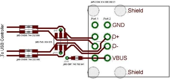
Figure 12: Protection of double USB port
Bill of Material:
In this application note the following parts are used:
TVS-Diodes WE-TVS:
824011: Protection of 2 I&O lines and VDD line: Size SOT23-5L | 2pF CI/O | 5V VRWM | 5A IPP
824015: Protection of 4 I&O lines and VDD line: Size SOT23-6L | 2pF CI/O | 5V VRWM | 5A IPP
ESD Suppressors WE-VE:
82307050029: Size 0402 | 0.2pF Ctyp | 5V VRWM | 17V VCL
82306050029: Size 0603 | 0.2pF Ctyp | 5V VRWM | 30V VCL
Common Mode Chokes WE-CNSW:
744232090: Size 1206 | 370mA IDC | 300 mRDC | 90W Impedance
Chip Bead Ferrites WE-CBF:
742792641: Size 0603 | 2 000mA IDC | 150 mRDC | 300W Impedance
USB-Connectors WR-COM:
61400826021: USB Typ A Connector | THT | Dual stacked
614004135023: USB Typ A Connector | THT | Vertical
I M P O R T A N T N O T I C E
The Application Note is based on our knowledge and experience of typical requirements concerning these areas. It serves as general guidance and should not be construed as a commitment for the suitability for customer applications by Würth Elektronik eiSos GmbH & Co. KG. The information in the Application Note is subject to change without notice. This document and parts thereof must not be reproduced or copied without written permission, and contents thereof must not be imparted to a third party nor be used for any unauthorized purpose.
Würth Elektronik eiSos GmbH & Co. KG and its subsidiaries and affiliates (WE) are not liable for application assistance of any kind. Customers may use WE’s assistance and product recommendations for their applications and design. The responsibility for the applicability and use of WE Products in a particular customer design is always solely within the authority of the customer. Due to this fact it is up to the customer to evaluate and investigate, where appropriate, and decide whether the device with the specific product characteristics described in the product specification is valid and suitable for the respective customer application or not.
The technical specifications are stated in the current data sheet of the products. Therefore the customers shall use the data sheets and are cautioned to verify that data sheets are current. The current data sheets can be downloaded at www.we-online.com. Customers shall strictly observe any product-specific notes, cautions and warnings.WE reserves the right to make corrections, modifications, enhancements, improvements, and other changes to its products and services.
WE DOES NOT WARRANT OR REPRESENT THAT ANY LICENSE, EITHER EXPRESS OR IMPLIED, IS GRANTED UNDER ANY PATENT RIGHT, COPYRIGHT, MASK WORK RIGHT, OR OTHER INTELLECTUAL PROPERTY RIGHT RELATING TO ANY COMBINATION, MACHINE, OR PROCESS INWHICHWE PRODUCTS OR SERVICES ARE USED. INFORMATION PUBLISHED BY WE REGARDING THIRD-PARTY PRODUCTS OR SERVICES DOES NOT CONSTITUTE A LICENSE FROM WE TO USE SUCH PRODUCTS OR SERVICES OR A WARRANTY OR ENDORSEMENT THEREOF.
WE products are not authorized for use in safety-critical applications, or where a failure of the product is reasonably expected to cause severe personal injury or death. Moreover, WE products are neither designed nor intended for use in areas such as military, aerospace, aviation, nuclear control, submarine, transportation (automotive control, train control, ship control), transportation signal, disaster prevention, medical, public information network etc. Customers shall inform WE about the intent of such usage before design-in stage. In certain customer applications requiring a very high level of safety and in which the malfunction or failure of an electronic component could endanger human life or health, customers must ensure that they have all necessary expertise in the safety and regulatory ramifications of their applications.
Customers acknowledge and agree that they are solely responsible for all legal, regulatory and safety-related requirements concerning their products and any use ofWE products in such safety-critical applications, notwithstanding any applicationsrelated information or support that may be provided by WE. CUSTOMERS SHALL INDEMNIFY WE AGAINST ANY DAMAGES ARISING OUT OF THE USE OF WE PRODUCTS IN SUCH SAFETY-CRITICAL APPLICATIONS.
USEFUL LINKS
Application Notes: http://www.we-online.com/app-notes
REDEXPERT Design Tool: http://www.we-online.com/redexpert
Toolbox: http://www.we-online.com/toolbox
Product Catalog: http://katalog.we-online.de/en/
DIRECT LINK:
ANP002: The Protection of USB 2.0 Applications
CONTACT INFORMATION
Würth Elektronik eiSos GmbH & Co. KG
Max-Eyth-Str. 1, 74638 Waldenburg, Germany
Tel.: +49 (0) 7942 / 945 – 0
Email: appnotes@we-online.de
Web: http://www.we-online.com
Top Comments