
APPLICATION NOTE

Extremely compact, Isolated Gate Driver PowerSupply for SiC-MOSFET (6 - 10 W)
ANP082 BY ANDREAS NADLER / ELEAZAR FALCO / EMIL NIERGES
1. Introduction
Wide bandgap power semiconductor devices like Silicon Carbide (SiC) MOSFETs are enjoying growing popularity in many modern power electronic applications like E-mobility and renewable energy. Their extremely fast switching speed capability helps to increase efficiency and reduce the overall size and cost of the system. However, fast switching together with high operating voltages and increasing switching frequencies presents important challenges to the gate driver system. Rugged galvanic isolation, compliance with safety standards, control signal noise immunity and EMI performance are just some of the most important aspects to consider. An optimal design of the isolated auxiliary supply providing the voltage and current levels to drive the SiC/GaN device is critical to help the full gate driver system meet the many requirements set by state-of-the-art applications.
2. Overview and requirements for gate control of HV SiC / GaN FET devices

Figure 1: Overview of a HV half-bridge control of the High-side & Low-side SiC-MOSFET.
In applications using SiC/GaN high-voltage semiconductor devices under hard-switching operation, galvanic isolation is a common requirement for safety and functional reasons, and depending on the application, a basic or a reinforced insulation will be required. The operating voltage, insulation material, pollution degree and the applicable regulatory standards set the minimum creepage and clearance distances as well as the dielectric isolation voltage requirement affecting the components placed across the isolation barrier. The high-speed isolated gate driver IC (e.g. TI UCC21520) and the transformer in the isolated auxiliary power supply (DC/DC Block in figure 1) both ‘bridge’ this isolation barrier, thus having to meet stringent safety and functional requirements.
Some of the latest SiC-MOSFET devices require typical gate voltages of +15 V for full turn-on and -4 V for reliable turn-off. For a GaN-FET usually only +5 V and 0 V are required respectively, although a small negative voltage can also be applied to ensure turn-off in presence of excessive gate voltage ringing. Please note that these values may vary depending on manufacturer. In figure 1, a half-bridge configuration is shown, and several of these stages are typically required in an inverter circuit to drive AC-motors in the kW range. Each SiC/GaN FET would require an independent gate driver stage with its own isolated auxiliary supply. This not only enables individual control of each SiC/GaN device, but also helps to keep the gate current loop small and local to the device, minimizing the adverse effects of parasitic loop inductance and ground bounce caused by the very high ΔI/Δt generated during the switching transition (figure 2 and figure 3).
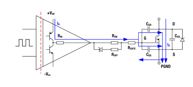
Figure 2: High ΔI/Δt current paths on turn-ON of SiC/GaN FET.
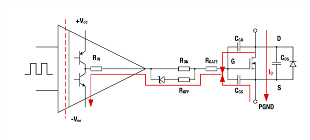
Figure 3: High ΔI/Δt current paths on turn-OFF of SiC/GaN FET.
Otherwise, this may cause uncontrolled turn-on/off of the MOSFET and thermal issues. Some SiC MOSFETs are designed with an additional low impedance Kelvin source connection (figure 4) for a gate current return path. This connection does not carry the high switching current and therefore has a lower interference potential than the source connection, which significantly improves gate driving. (e.g. Infineon IMZ120R045M1 1200 V / 52 A).

Figure 4: Kelvin connections and critical parasitic inductances in a half-bridge configuration.
Regarding the auxiliary supply, it should be compact with its output capacitors (with minimal ESL and ESR) placed very close to the gate driver and SiC/GaN device to minimize the gate current loop and associated parasitic effects.
3. Requirements of the Isolated Gate Driver Power Supply for SiC-MOSFETs
There is currently a large selection of compact, isolated 1 – 2 W DC/DC converters available on the market. For a SiC-MOSFET like the Infineon IMZ120R045M1 1200 V / 52 A, up to 1 W power requirement per device can be estimated (see example calculation (1)). However, an application with over 5 kW load power would require the use of either a SiC-MOSFET module (e.g. ROHM BSM600D12P3G001 1200 V / 600 A) or alternatively several discrete SiC-MOSFETs in parallel (current sharing). In a module solution, several semiconductor dies are paralleled to form the final SiC-MOSFET. This technique reduces the effective RDS(ON) but results in a very high "Total Gate Charge", which places a higher power requirement on the gate driver system power supply (example calculation (2)). Above 2 W of power, there is only a very limited selection of off-the-shelf isolated DC-DC converter modules, which despite their convenience, are often large, weighty, expensive and with efficiencies lining under 79%.
PGate = PDriver + (QGate ⋅ FSW ⋅ ΔVGate)
PGate | Total power required to drive the SiC device gate |
| PDriver | Power loss in the gate driver section (approx. 0.3 W) |
| QGate | Total Gate Charge value (from datasheet) |
| FSW | Maximum switching frequency |
| △VGate | Maximum voltage swing at the gate from –Vee to + Vdd (e.g. -4 V to +15 V = 19 V) |
Example calculation (1) with Infineon IMZ120R045M1 1200 V / 52 A:
PGate = 0.3 W + (62 nC ⋅ 100 kHz ⋅ 19 V) = 0.42 W
Example calculation (2) with ROHM BSM600D12P3G001 1200 V / 600 A:
PGate=0.3W+(1900nC⋅100kHz⋅19V)=3.91W
The SiC-MOSFET modules currently available feature a total gate charge of 3000 nC. With an increase in the switching frequency or load power (requiring more paralleled SiC-devices with the corresponding increase of the total gate charge), 6 - 10 W of driver system power can be expected for the most demanding present and near-future applications.
Amongst the solutions available meeting the above specification, one of the best 6 W isolated converter modules on the market currently has the following specification:
| 9 – 18 V |
| +15 V / -5 V @ 6 W |
| 40 x 28 x 9 mm |
| 76 - 79% |
| 15 pF |
| 12 g |
| 800 V |
Efficiency, weight and especially the parasitic coupling capacitance are often critical parameters in high-performance systems. Especially at higher switching frequencies of the converters and the resulting very steep switching edges, the harmonics must be capacitively decoupled between the converter output stage/gate driver and the system power supply, i.e. from the DC-DC converter.
The parasitic capacitance ( CP ) between primary and secondary sides is mainly set by the interwinding capacitance of the DC/DC power transformer device. With latest SiC-MOSFETs switching at ΔU/Δt slew-rates of 100 kV/us, 10 pF parasitic capacitance across the barrier would cause a peak displacement current of 1 A which is coupled by the switching transistor across the isolation barrier. A high dielectric
displacement current degrades the insulation barrier in the long run, disturbs the control signals and leads to common mode currents in the corresponding device, which can be seen as typical EMC problems.
IP=CP×△U△t
IP electrical displacement current
CP parasitic coupling capacitance
It is recommended to keep CP in the auxiliary supply below 10 pF.
Würth Elektronik has addressed all these requirements and it is presenting an optimized solution with its new SiC gate driver power supply reference design.
4. Würth Elektronik Solution up to 6W (10W)
The high-performance bipolar isolated auxiliary power supply design of Würth Elektronik features the following specifications:
- Input voltage range: 9 - 18 V
- Output voltage: bipolar +15 V / -4 V or Unipolar 15 - 20 V
- Power up to 6 W
- Peak efficiency of up to 86% (83% @ 6 W)
- Parasitic coupling capacitance less than 7 pF
- Size: 27 x 14 x 14 mm (L x W x H)
-> Over 50% smaller than similar DC/DC converters currently on the market
- Weight: < 4 g
- Basic insulation for VBus: 800 V
- 4000 Vrms insulation voltage Pri-sec
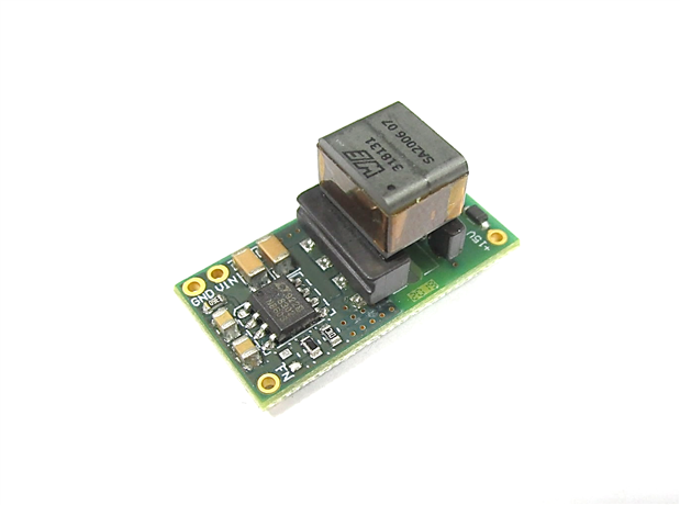
Figure 5: Würth Elektronik reference design for a compact, isolated DC/DC converter for HV SiC/GaN/IGBT Gate Driver
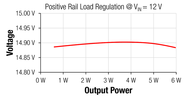
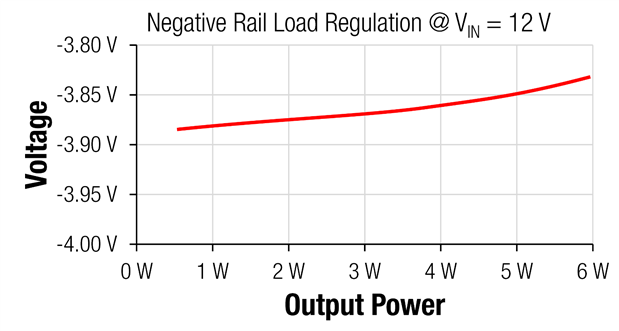
Figure 6: Voltage of Positive and Negative rails versus load power (@ VIN (nominal) = 12 V)
In addition to the controller (Analog Devices), the key component in the design is the new power transformer (WE-AGDT-750318131). A compact EP7 customized package was used and optimized to meet the following requirements:
- Wide Input Voltage Range: 9 - 36 V
- High saturation current of 4.5 A
- Very low interwinding capacitance typ. 6.8 pF
- Very low leakage inductance for highest efficiency
- SMD Pick & Place ready
- Creepage & Clearance distance min. 5 mm
- Safety Standard IEC-62368-1, IEC-61558-2-16
- Basic Insulation
- Dielectric Isolation min. 4 kV AC
- Temperature Class B 155 °C
- AEC-Q200 Qualification
A comprehensive reference design document RD001 is available for download (6 W bipolar solution for SiC-MOSFET), alongside with the corresponding PCB Layout design files.
Please note that the power capability can be easily scaled to 10 W with an EP10 transformer core and appropriate uprating of some components.
The new WE-AGDT Gate Driver Transformer series from Würth Elektronik features six different transformers, each of them optimized for different specifications and their own reference design. These transformers offer flexibility, ease of use and a combination of bipolar and unipolar output voltage rail options, covering the gate-drive requirements not only of state-of-the-art SiC-MOSFETs, but also GaN-FETs and widespread silicon IGBT and power-MOSFET devices.
5. Summary
With the new transformer series WE-AGDT, Würth Elektronik is demonstrating its innovative strength addressing the future challenges in the field of power electronics. For the first time, the developer has the possibility to easily implement a compact and efficient gate driver supply with up to 6 W output power capability and top performance.
IMPORTANT NOTICE
The Application Note is based on our knowledge and experience of typical requirements concerning these areas. It serves as general guidance and should not be construed as a commitment for the suitability for customer applications by Würth Elektronik eiSos GmbH & Co. KG. The information in the Application Note is subject to change without notice. This document and parts thereof must not be reproduced or copied without written permission, and contents thereof must not be imparted to a third party nor be used for any unauthorized purpose.
Würth Elektronik eiSos GmbH & Co. KG and its subsidiaries and affiliates (WE) are not liable for application assistance of any kind. Customers may use WE’s assistance and product recommendations for their applications and design. The responsibility for the applicability and use of WE Products in a particular customer design is always solely within the authority of the customer. Due to this fact it is up to the customer to evaluate and investigate, where appropriate, and decide whether the device with the specific product characteristics described in the product specification is valid and suitable for the respective customer application or not.
The technical specifications are stated in the current data sheet of the products. Therefore the customers shall use the data sheets and are cautioned to verify that data sheets are current. The current data sheets can be downloaded at www.we-online.com. Customers shall strictly observe any product-specific notes, cautions and warnings. WE reserves the right to make corrections, modifications, enhancements, improvements, and other changes to its products and services.
WE DOES NOT WARRANT OR REPRESENT THAT ANY LICENSE, EITHER EXPRESS OR IMPLIED, IS GRANTED UNDER ANY PATENT RIGHT, COPYRIGHT, MASK WORK RIGHT, OR OTHER INTELLECTUAL PROPERTY RIGHT RELATING TO ANY COMBINATION, MACHINE, OR PROCESS IN WHICH WE PRODUCTS OR SERVICES ARE USED. INFORMATION PUBLISHED BY WE REGARDING THIRD-PARTY PRODUCTS OR SERVICES DOES NOT CONSTITUTE A LICENSE FROM WE TO USE SUCH PRODUCTS OR SERVICES OR A WARRANTY OR ENDORSEMENT THEREOF.
WE products are not authorized for use in safety-critical applications, or where a failure of the product is reasonably expected to cause severe personal injury or death. Moreover, WE products are neither designed nor intended for use in areas such as military, aerospace, aviation, nuclear control, submarine, transportation (automotive control, train control, ship control), transportation signal, disaster prevention, medical, public information network etc. Customers shall inform WE about the intent of such usage before design-in stage. In certain customer applications requiring a very high level of safety and in which the malfunction or failure of an electronic component could endanger human life or health, customers must ensure that they have all necessary expertise in the safety and regulatory ramifications of their applications. Customers acknowledge and agree that they are solely responsible for all legal, regulatory and safety-related requirements concerning their products and any use of WE products in such safety-critical applications, notwithstanding any applications-related information or support that may be provided by WE.
CUSTOMERS SHALL INDEMNIFY WE AGAINST ANY DAMAGES ARISING OUT OF THE USE OF WE PRODUCTS IN SUCH SAFETY-CRITICAL APPLICATIONS.
USEFUL LINKS
Application Notes: http://www.we-online.com/app-notes
REDEXPERT Design Tool: http://www.we-online.com/redexpert
Component Selector: http://www.we-online.com/component-selector
Toolbox: http://www.we-online.com/toolbox
Product Catalog: http://katalog.we-online.de/en
DIRECT LINK
ANP082: Extremely compact, Isolated Gate Driver PowerSupply for SiC-MOSFET (6 - 10 W)
CONTACT INFORMATION
Würth Elektronik eiSos GmbH & Co. KG
Max-Eyth-Str. 1, 74638 Waldenburg, Germany
Tel.: +49 (0) 7942 / 945 – 0
Email: appnotes@we-online.de