
SUPPORT NOTE
Contact debounce circuit for switches

SN015 BY ALEXANDRE CHAILLET / EVELYN HUANG
1 Introduction
Würth Elektronik offers a wide range of switch products. These products are used for many applications to simply open and close electronic circuits.
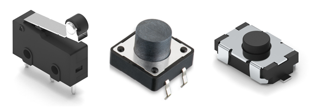
Figure 1: Part of the WE-switch portfolio
The switching function is mainly mechanical, but many switches are operating like an analog-digital interface for modern electronic circuits, with clearly defined voltage levels for logic 0 and logic 1. But anyone who has built an application with a tact or detector switch with a fast responding electronic circuit may be wondering why the circuit is not working properly. The reason may be what is called contact bouncing (also known as chattering). There are possibilities to eliminate the effects of this phenomena and this application note proposes a circuit to avoid this common issue.
2 What is contact bounce
2.1. Principle of switching mechanics
We naturally have the impression that the contact in a switch is immediate and firm.
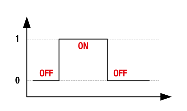
Figure 2: Idealized graph of a switched signal
However, the “reality” looks a little bit different.
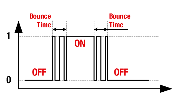
Figure 3: Idealized graph of a “real” switched signal
At each switch position, contact between electrically conductive points is established or separated by means of movable mechanical elements.
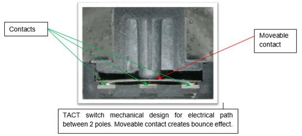
Figure 4: TACT switch design
Typically, spring components are used as transmitters of the nominal state, either as a metal plate or as a coiled spring, which have a certain mass and thus a certain moment of inertia. When these small components are set in motion for a change of state, they are accelerated until they have reached the desired position. There, they experience a reverse acceleration due to the principles of elastic shock and their spring characteristics. This effect occurs several times in succession until the movement is completely damped. As the damping factor is high and the moment of inertia is small, the effect itself typically only takes a few microseconds. This is not problematic for power circuits but this rebounding signal on status change creates bad transitions for a digital input. During the status change, the electronic signal has an unstable or better said undefined status. For a logic IC this can be really problematic, as it needs a clean defined signal. A microcontroller reading the port may miss the changed state if read at the wrong moment. Therefore a solution is needed to generate a clear output from the switch and we will take a look at a switch debounce circuit to solve this problem.
2.2. Applicable products
Debounce time is given in the product datasheet. Würth Elektronik defines bounce time as the time between when the product is mechanically switched and when it is fully electrically switched.
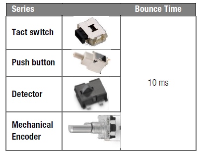
Table 1: Applicable products for debounce circuit
3 Debounce circuit
In the following we will add some components to create a low pass filter circuit to see the influence on the signal output.
3.1. Adding a filter
The base switch circuit with no debounce compensation circuit looks like the following:
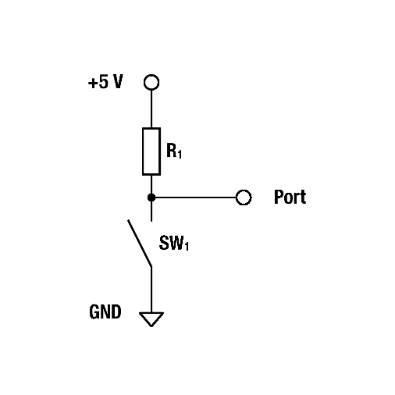
Figure 5: Switch circuit without debounce circuit
Classical values for resistor are R1 = 1 kΩ to 10 kΩ and VCC = 5 V.
Pushing the switch gives the following switching response that shows the bounce effect:
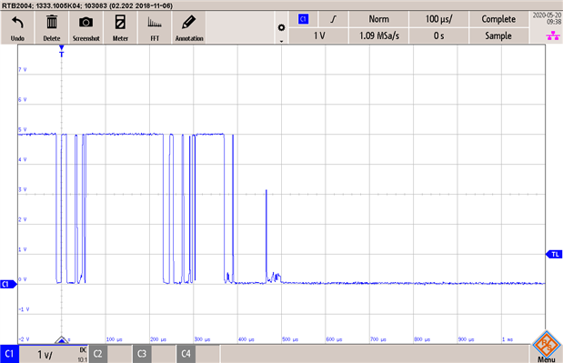
Figure 6: Output without debounce circuit during high to low transition
To solve this bounce in the VOUT signal, a different electronic circuit is proposed. The following electronic circuit, a simple RC filter is one of the cheapest and simplest to realize. When the switch is open the capacitor charges through R1+R2 which causes the voltage to rise more slowly. When the switch is closed, the capacitor is discharged through R2 at a controlled rate.
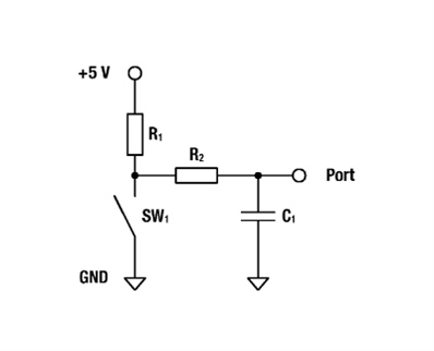
Figure 7: Switch circuit with a basic debounce circuit
When the components are selected carefully, the switch bouncing is absorbed during the charging or discharge period providing a smooth transition.
To calculate the value of capacitor and resistors, we need to know the following time constant formula applicable for this schematic:
ꞇ = (R1+R2)×C1 (1)
ꞇ : time constant in s
R : resistor value in Ω
C : capacitance value in F
The time constant is a balance between the needs to debounce the switch and the required response time of the circuit. During one time constant the voltage will rise to 63% of its final value or fall to 37% of its final value. In both cases, 99% is reached after five time constants.
3.2. Calculation example:
Fixed conditions
- Bounce time: specifications give 10 ms
- R1 is chosen to limit current, we take the classical value of 1 kΩ.
- R2: we choose two standard values for debouncing: 10 kΩ and 47 kΩ.
- Supply Voltage is 5 VDC
Therefore, calculation gives two capacitance values:
C1=τR1+R2 (2)
And then we propose two value ranges for this circuit:
- Solution 1 : R1 = 1 kΩ, R2 = 10 kΩ, C1 = 1 μF
- Solution 2 : R1 = 1 kΩ, R2 = 47 kΩ, C1 = 220 nF
For both circuits, the answer becomes like following:
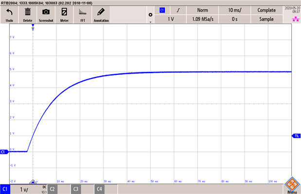
Figure 8: Output with debounce circuit during low to high transition
Note: Resistance and capacitance values, could vary according to customer circuit design
The value of UOUT vs. time is given by the next formula
UOUT=UIN×(1−e−tꞇ ) (3)
We see that at t = ꞇ, we reach a value of UOUT ≈ 63 % UIN.
In our example UOUT is at 63 % (3.15 V) of its final value (5.0 V) after 10 ms.
3.3. Adding a diode
It is possible to control the charge time and discharge time separately by adding a diode across R2. This allows for a faster transition time to charge the capacitor using R1 and D2 and a different discharge time using only R2, as in this case the diode is blocking.
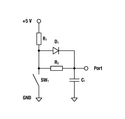
Figure 9: Adding a diode to the schematic
3.4. Adding a buffer
The user must also be aware the digitial logic is defined with zero being below a certain voltage (ie. 0.8 V) and one being above a certain voltage (ie. 2.5 V). The values between are undefined. If the application cannot support the undefined values a Schmitt trigger buffer with hysteresis may be required. A circuit with different switch-on and switch-off times and additional hysteresis is shown in figure 10. The response time of the circuit may have to be coordinated with the sampling time of the microcontroller.
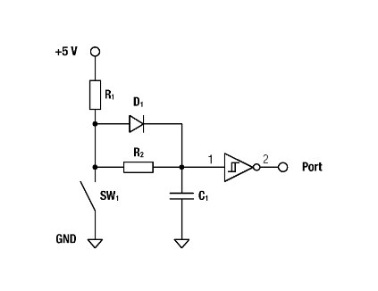
Figure 10: A schmitt trigger enures stable and defined voltage values
3.5. Transient protection
If the switch is located far away or at the end of a long wire, there will likely be a need for protection against overvoltage, ESD or other transients. This can be as simple as a ferrite bead and TVS diode in front of the input circuitry.
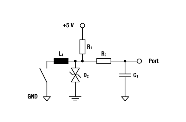
Figure 11: Adding a ferrite bead and TVS diode for overvoltage protection
4 Summary
Using mechanical switch products for signals gives a bounce effect that may cause short periods of unstable signal for an electronic circuit. Würth Elektronik switches have a bounce time of up to 10 ms, which should be considered, depending on the application. Therefore, the proposed filter in figure 7 can help to reduce this phenomena. The filter can also be upgraded with additional components for more refined signal conditioning and overvoltage protection.
A. Appendix
A.1. References
- Brander, T., Gerfer, A., Rall, B., Zenkner, H., Trilogy of Magnetics, 5th ed., Waldenburg, 2018
- Gerfer, A., Jugy, R., Mroczkowski R., Robok, T., Trilogy of Connectors, 3th ed., Waldenburg, 2015
IMPORTANT NOTICE
The Application Note is based on our knowledge and experience of typical requirements concerning these areas. It serves as general guidance and should not be construed as a commitment for the suitability for customer applications by Würth Elektronik eiSos GmbH & Co. KG. The information in the Application Note is subject to change without notice. This document and parts thereof must not be reproduced or copied without written permission, and contents thereof must not be imparted to a third party nor be used for any unauthorized purpose.
Würth Elektronik eiSos GmbH & Co. KG and its subsidiaries and affiliates (WE) are not liable for application assistance of any kind. Customers may use WE’s assistance and product recommendations for their applications and design. The responsibility for the applicability and use of WE Products in a particular customer design is always solely within the authority of the customer. Due to this fact it is up to the customer to evaluate and investigate, where appropriate, and decide whether the device with the specific product characteristics described in the product specification is valid and suitable for the respective customer application or not.
The technical specifications are stated in the current data sheet of the products. Therefore the customers shall use the data sheets and are cautioned to verify that data sheets are current. The current data sheets can be downloaded at www.we-online.com. Customers shall strictly observe any product-specific notes, cautions and warnings. WE reserves the right to make corrections, modifications, enhancements, improvements, and other changes to its products and services.
WE DOES NOT WARRANT OR REPRESENT THAT ANY LICENSE, EITHER EXPRESS OR IMPLIED, IS GRANTED UNDER ANY PATENT RIGHT,
COPYRIGHT, MASK WORK RIGHT, OR OTHER INTELLECTUAL PROPERTY RIGHT RELATING TO ANY COMBINATION, MACHINE, OR PROCESS IN WHICH WE PRODUCTS OR SERVICES ARE USED. INFORMATION PUBLISHED BY WE REGARDING THIRD-PARTY PRODUCTS OR SERVICES DOES NOT CONSTITUTE A LICENSE FROM WE TO USE SUCH PRODUCTS OR SERVICES OR A WARRANTY OR ENDORSEMENT THEREOF.
WE products are not authorized for use in safety-critical applications, or where a failure of the product is reasonably expected to cause severe personal injury or death. Moreover, WE products are neither designed nor intended for use in areas such as military, aerospace, aviation, nuclear control, submarine, transportation (automotive control, train control, ship control), transportation signal, disaster prevention, medical, public information network etc. Customers shall inform WE about the intent of such usage before design-in stage. In certain customer applications requiring a very high level of safety and in which the malfunction or failure of an electronic component could endanger human life or health, customers must ensure that they have all necessary expertise in the safety and regulatory ramifications of their applications. Customers acknowledge and agree that they are solely responsible for all legal, regulatory and safety-related requirements concerning their products and any use of WE products in such safety-critical applications, notwithstanding any applications-related information or support that may be provided by WE.
CUSTOMERS SHALL INDEMNIFY WE AGAINST ANY DAMAGES ARISING OUT OF THE USE OF WE PRODUCTS IN SUCH SAFETY-CRITICAL APPLICATIONS.
USEFUL LINKS
Application Notes: http://www.we-online.com/app-notes
REDEXPERT Design Tool: http://www.we-online.com/redexpert
Component Selector: http://www.we-online.com/component-selector
Toolbox: http://www.we-online.com/toolbox
Product Catalog: http://katalog.we-online.de/en
DIRECT LINK
SN015: Contact debounce circuit for switches
CONTACT INFORMATION
Würth Elektronik eiSos GmbH & Co. KG
Max-Eyth-Str. 1, 74638 Waldenburg, Germany
Tel.: +49 (0) 7942 / 945 – 0
Email: appnotes@we-online.de


