
The Behavior of Electromagnetic Radiation of Power Inductors in Power Management
ANP047 by Ranjith Bramanpalli
1. Introduction
DC-DC converters are widely used in power management applications and the inductor is one of the key components (Figure 1). The usual focus is on electrical performance characteristics such as RDC, RAC and core losses. But, the electro-magnetic radiation characteristics can often be overlooked.

Figure 1: Typical DC-DC Converter
Power inductors in switch mode power supplies (SMPS) can be made of various core materials and different types of windings (coils). Inductors can also be classified into three types; unshielded, semi-shielded and shielded. Different types of inductor have advantageous and disadvantageous characteristics that permit or limit their range of application.
Due to the switching action in SMPS, AC voltage/current is produced over the inductor. Since, an inductor can, in effect, operate as a transmitting loop antenna, the electromagnetic radiation depends on a number of factors. These include the source properties such as core material, shielding material and the orientation of the start of the winding amongst others.
Electromagnetic radiation of an inductor in the low frequency spectrum range (100 kHz to 30 MHz), which is caused by the switching frequency and harmonics, is dependent on whether the inductor is shielded and the winding properties. Whereas, in the high frequency spectrum range (30 MHz to 1 GHz), where emissions are caused by ringing frequencies and their harmonics, the electromagnetic radiation is more dependent on the shielding characteristics of the core material, switching frequency and transitions of the switching converter.
2. Electro-Magnetic (EM) Radiation
The inherent design and operation of inductor(s) in DC/DC converters leads to unfavorable attributes which are comparable to that of a loop antenna. The AC voltage and current in the inductor produces electric (E-field) and magnetic (H-field) fields which propagate away from the source at right angles to one another.
Near to the loop antenna (source), the characteristics of the fields (E and H) are determined by the behavior of the source characteristics (switching frequency, transitions). However, far from the source, the properties of the field are determined by the medium it propagates through. These separate yet interconnected phenomena can therefore be divided into two regions; the near-field and the far-field as shown in Figure 2. The area within λ /2π of the source is defined as the near-field whereas further than this is defined as far-field radiation.
In the near-field, the E and H-fields must be considered separately as the ratio between the two fields is not constant. The ratio E/H is also called wave impedance. However, in the far-field these fields combine to form a plane wave. Hence, individual electric (E) and magnetic (H) fields are only discussed in the context of near-field. If the source has high current and low voltage, the magnetic field is said to be dominant whereas if the source has low current and high voltage then the electric is said to be dominant.

Figure 2: Near and far-field region(s) spread spectrum
For a loop antenna, magnetic field near the source is high resulting in a low wave impedance near the antenna. As the distance from the source increases, the magnetic field declines simultaneously generating an electric field perpendicular to the direction of the H-field. The magnetic field attenuates at a rate of (1/r)³ and the electric field attenuates at a rate of (1/r)² when moving away from the source where r is the distance.
For a straight wire antenna, the wave impedance is high, hence the electric field is dominant near the source and the attenuation characteristics are entirely opposite to that of loop antenna.
2.1. EM radiation behavior of Unshielded, Semi-Shielded and Shielded Inductors
As we have seen in the previous section, radiation from inductors in DC/DC converters is no triviality, especially when considering the type and proximity of surrounding components and their susceptibility to magnetic coupling. As engineers have become more mindful of this source of potential EMI, component manufactures have responded by offering ranges of inductors that are shielded and semi-shielded in addition to conventional unshielded inductors. Shielded inductors are manufactured to fully encapsulate the coil in a form of magnetic shielding. With unshielded inductors, the coil windings are typically exposed or otherwise magnetically not shielded. These are generally the worst offenders from an EMI perspective due to the unhindered propagation of EM fields. In semi-shielded inductors magnetic materials are usually glued over the exposed windings with epoxy resin.


Figure 3: Test setup and block diagram
Each type of inductor has its own advantages and disadvantages. The main advantage of the shielded inductor is its relatively low emissions when compared to semi-shielded or shielded inductors (Figure 4).

Figure 4: Magnetic radiation of unshielded, semi-shielded and shielded inductors
But as most electrical engineers know, a fine balancing act must be maintained when a new design is in development. Increasing a desirable characteristic can often increase undesirable characteristics which are ultimately restrained by the overall project requirements. One of those restraints is unescapably size. Shielded inductors, when compared to the same Inductance value required of unshielded inductors and of the same dimensions, have lower DC-resistance and lower saturation. Naturally, this would direct the less experienced engineer to select an unshielded inductor which is smaller and has higher saturation current capability. But this will ultimately lead to a myriad of electromagnetic interference and compatibility issues which cannot be compromised.
Würth Elektronik is one of the few companies to offer semi-shielded inductors which walk the fine balancing line between space requirements, electrical characteristics and EMI. Semi-shielded inductors are particularly suited to applications where components close to the inductor are not severely sensitive to radiation. The excellent saturation characteristics of the WE-LQS semi shielded inductor size 8040 (744 040 841 00) are presented in Figure 5 and compared with shielded inductor WE-PD size 7345 (744 777 10) and unshielded inductor WE-PD2 size 7850 (744 775 10).

Figure 5: Saturation characteristics of shielded, semi-shielded and unshielded inductor
2.2. EM Radiation due to the Influence of Start of the Winding in an Inductor
One EMI consideration that can easy be overlooked is the orientation of the start of the coil winding. The 'dot' on the inductor package represents the start of winding (Figure 6). It is important to connect the dotted end of the inductor closest to the switch node as this is the end that will undergo the most dV/dt and thus generate the most interference. In this way, the AC flux from switch node switching will be shielded by the outer windings. If the non-dot end is connected to the switch node, AC flux voltages are present on the outside winding layer which can cause unacceptable levels of electric or capacitive coupling.


Figure 6: WE-XHMI and WE-PD2 with the 'dot' identifying the location of the start of the winding
Magnetically shielded inductors are effective at shielding H-field dominant radiation but may not be able to shield E-field dominant radiation in all conditions. Effective E-shielding depends on the material properties and complex permeability. The higher the thickness and permeability of the core material, the more effective the inductor will be at shielding the E-field.
As an example, the E-field emissions of a Würth Elektronik shielded inductor was measured with a WE-LHMI (744 373 680 22). The transistor of the converter was operating at 400 kHz producing the fundamental resonance and subsequent harmonics. The spectrum clearly shows that emissions from the inductor re up to 8 dB lower when the dotted end of the inductor is connected to the switch node (Figure 7).It is, therefore, highly recommended to use the inductor in the correct orientation. The H-field emissions, however, are unaffected by the change of orientation of the inductor (Figure 8).
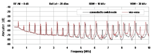
Figure 7: E-field of the inductor’s start of winding connected to the switch node and vice-versa

Figure 8: H-field of the inductor’s start of winding connected to the switch node and vice-versa
2.3. EM radiation due to the Influence of switching transitions
There cannot be electromagnetic interference if either the source, medium or the victim is not present. As switching frequencies increase, DC/DC converters also employ faster rise and fall times of the switching device to keep switching losses low. But this creates steep switch-node transitions, accompanied by switch-node ringing and spikes (Figure 9). The resulting switch-node ringing and the inductor voltage waveform is shown in Figure 10.


Figure 9: V_DS of Buck converter on the left and switch node ringing during turn on of S1 on the right


Figure 10: Voltage waveform over the storage Inductor of buck converter on the left and resulting ringing on the inductor during turn on of S1 on the right Note: Input: 12V, Output: 5V, 5A, Switching Frequency: 400 kHz, Ringing Frequency: 128MHz
Because of switch node ringing, fast transitions and high switching frequency, it is necessary to choose an appropriate inductor for achieving electromagnetic compatibility. Typically, the ringing frequency is in the 100 to 200 MHz range. The effectiveness of attenuating emissions at these frequencies very much depends on the inductors properties, most notably, the core material (Figure 11) and thickness.
Usually, iron powder and metal alloy powder inductors have less E-field shielding effectiveness at frequencies above 1 MHz. Here MnZn and NiZn have better performance at higher switching frequencies.
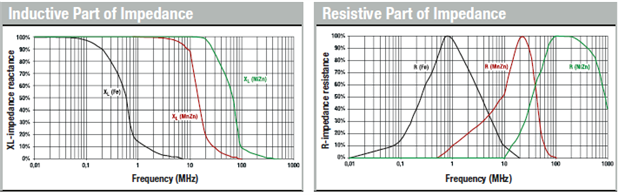
Figure 11: Resistive and inductive characteristics of widely used core materials- Iron powder, MnZn and NiZn.
The effect on the radiation of H and E-fields when changing the core material may be seen below (Figure 12 and Figure 13). The DC-DC converter used for the testing is switching at 400 kHz and ringing frequency on the switch node is about 180 MHz. As demonstrated, an inductor with a NiZn core (WE-PD 744 771 402 2) is much more successful at limiting H and E-field radiation at higher switching frequencies than an Inductor with MnZn core (WE-HCF 744 363 022 0).

Figure 12: H-field comparison of iron powder (WE-LHMI), MnZn (WE-HCF) and NiZn (WE-PD) core material
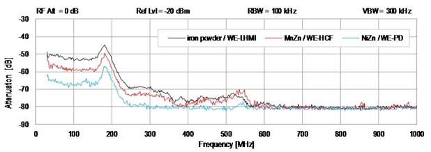
Figure 13: E-field comparison of iron powder (WE-LHMI), MnZn (WE-HCF) and NiZn (WE-PD) core material
3. Shielding
Every core material has inherent advantages and disadvantages which are particularly suited to a specific application. In these circumstances where a core material cannot be substituted, external solutions may be necessary to mitigate emissions. For example, inductors made of iron powder/metal alloy core material have excellent saturation characteristics and can be made in extremely small sizes but have limited shielding characteristics at frequencies above 1 MHz. Hence, to shield the emissions caused by the ringing frequency caused by a fast switching transition time, external shielding may be required to ensure electromagnetic compatibility. Metal and magnetic shielding solutions can be optimized based on the application.
Metal shielding materials are made of copper, aluminum, metal alloys and composite mixtures. Metal shielding usually consists of an enclosure that is attached over the source to reflect or absorb the noise. The thickness and type of material can be chosen based upon shielding effectiveness, frequency (Figure 14) and cost. Interestingly, some iron powder inductor manufacturers are integrating a metal bridge on the top of the inductor to improve shielding performance. However, this approach is less advantageous as it may first appear as these inductors are not as flexible to design and emission requirements as they have a limited effect at a constrained range of switching frequencies and fixed source properties.
Alternatively, magnetic shielding can be achieved using magnetic materials or µ-metals and their effectiveness are dependent on material permeability, impedance and thickness. The material characteristics are similar to those shown in figure 10.


Figure 14: Absorption and reflection characteristics of metal shielding
3.1. Effect of Shielding in the near-field
As mentioned earlier, the switch node ringing frequency on one demo-board is ≈130 MHz and on the other demo-board it is ≈ 180 MHz. Since the advantages of iron powder and metal alloy inductors cannot be compromised most of the time, Würth Elektronik offers a huge variety of metal and µ-metal shielding materials such as copper tape, various composite metal shielding cabinets with and without vents, NiZn and ferrite plates, etc. These products offer flexible and adaptable solutions that are suitable for specific design restraints and can be selected for the particular range of frequencies where attenuation is required (Figure 14). For example, the effectiveness of metal shielding of a Würth Elektronik WE-LHMI iron powder inductor is demonstrated by a 10 dB reduction in E-field emissions (Figure 16).
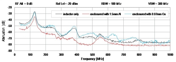
Figure 15: H-field comparison of iron powder (WE-LHMI) without additional shielding, with 1.5mm Aluminum enclosure and with 0.07mm copper tape
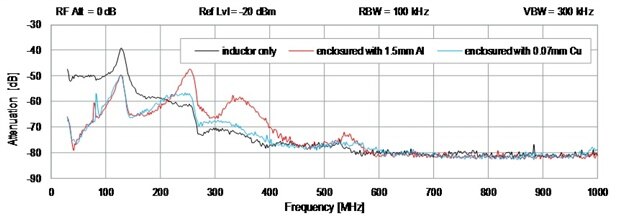
Figure 16: E-field comparison of iron powder (WE-LHMI) without additional shielding, with 1.5mm Aluminum enclosure and with 0.07mm copper tape
3.2. Effect of Shielding in the far-field
The effectiveness of shielding is not only limited to near field radiation. Notable reductions in far-field emissions can also be achieved using metal and ferrite solutions. The same demo-board was tested in the EMI chamber for far-field radiation. The value of enclosing an iron powder core inductor with a 1.5 mm thick aluminum shield is demonstrated below (Figure 17 and Figure 18) where the ringing frequency has been substantially reduced. In addition, attenuation was also notable over the whole frequency range including harmonics. Similarly, the addition of adding a 3 mm thick ferrite plate has a similar effect when placed on the iron powder inductor (Figure 19).
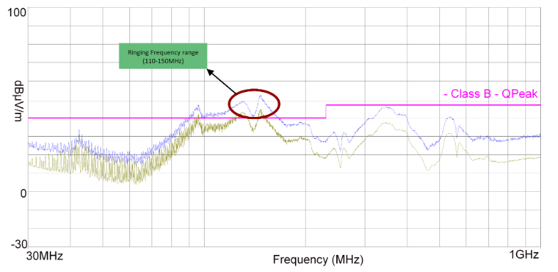
Figure 17: Far-field electro-magnetic radiation of the system, where the iron powder inductor is part of it

Figure 18: Far-field testing of the system with Aluminum enclosure on the inductor

Figure 19: Far-field testing of the system with 3mm ferrite plate on the top of the inductor
4. Summary
EM radiation is an incredibly vast and intricate topic as seemingly small variations in any one parameter can influence emission sources and therefore the near-field and far-field characteristics. The characterization of the near-field can be a complicated and lengthy process because of the necessity of many experiments and observations to fully comprehend and resolve EMI issues.
Additionally, the move towards high switching frequencies for higher power densities and better efficiency, as the availability of new technologies in Mosfets becomes readily available (GaN, SiC), further necessitates consideration and control of emissions. When switching at higher frequencies the usual approach for power magnetics is no longer valid. Würth Elektronik completely understands the necessity to address and is fully prepared to support with issues that arise due to changing technologies, designs and parameters.
Designing one specific inductor which is valid for only few conditions is not the WE way. A small change in the switching device can affect the source characteristics of the inductor dramatically. Specific components for a specific design for a specific application is required. For this reason, WE offers a wide variety of products together with unparalleled levels of support and technical assistance to ensure your device meets EMI standards.
5. BOM
Description | Size | Value | Order Code | Farnell Order Code |
WE-PD SMD Shielded Power Inductor | 7345 |
| 2763435 | |
WE-LQS SMD Power Inductor | 8040 |
| 2431553 | |
WE-PD2 SMD Power Inductor | 7850 |
| 1636035 | |
WE-PD SMD Shielded Power Inductor | 1050 |
| 2082672 | |
WE-HCF SMD High Current Inductor | 2013 |
| 1869756 |
6. References
- Electromagnetic Compatibility Engineering by Henry W. OTT
- http://www.we-online.com/app-notes
IMPORTANT NOTICE
The Application Note is based on our knowledge and experience of typical requirements concerning these areas. It serves as general guidance and should not be construed as a commitment for the suitability for customer applications by Würth Elektronik eiSos GmbH & Co. KG. The information in the Application Note is subject to change without notice. This document and parts thereof must not be reproduced or copied without written permission, and contents thereof must not be imparted to a third party nor be used for any unauthorized purpose.
Würth Elektronik eiSos GmbH & Co. KG and its subsidiaries and affiliates (WE) are not liable for application assistance of any kind. Customers may use WE’s assistance and product recommendations for their applications and design. The responsibility for the applicability and use of WE Products in a particular customer design is always solely within the authority of the customer. Due to this fact it is up to the customer to evaluate and investigate, where appropriate, and decide whether the device with the specific product characteristics described in the product specification is valid and suitable for the respective customer application or not.
The technical specifications are stated in the current data sheet of the products. Therefore the customers shall use the data sheets and are cautioned to verify that data sheets are current. The current data sheets can be downloaded at www.we-online.com. Customers shall strictly observe any product-specific notes, cautions and warnings. WE reserves the right to make corrections, modifications, enhancements, improvements, and other changes to its products and services.
WE DOES NOT WARRANT OR REPRESENT THAT ANY LICENSE, EITHER EXPRESS OR IMPLIED, IS GRANTED UNDER ANY PATENT RIGHT, COPYRIGHT, MASK WORK RIGHT, OR OTHER INTELLECTUAL PROPERTY RIGHT RELATING TO ANY COMBINATION, MACHINE, OR PROCESS IN WHICH WE PRODUCTS OR SERVICES ARE USED. INFORMATION PUBLISHED BY WE REGARDING THIRD-PARTY PRODUCTS OR SERVICES DOES NOT CONSTITUTE A LICENSE FROM WE TO USE SUCH PRODUCTS OR SERVICES OR A WARRANTY OR ENDORSEMENT THEREOF.
WE products are not authorized for use in safety-critical applications, or where a failure of the product is reasonably expected to cause severe personal injury or death. Moreover, WE products are neither designed nor intended for use in areas such as military, aerospace, aviation, nuclear control, submarine, transportation (automotive control, train control, ship control), transportation signal, disaster prevention, medical, public information network etc. Customers shall inform WE about the intent of such usage before design-in stage. In certain customer applications requiring a very high level of safety and in which the malfunction or failure of an electronic component could endanger human life or health, customers must ensure that they have all necessary expertise in the safety and regulatory ramifications of their applications. Customers acknowledge and agree that they are solely responsible for all legal, regulatory and safety-related requirements concerning their products and any use of WE products in such safety-critical applications, notwithstanding any applications-related information or support that may be provided by WE. CUSTOMERS SHALL INDEMNIFY WE AGAINST ANY DAMAGES ARISING OUT OF THE USE OF WE PRODUCTS IN SUCH SAFETY-CRITICAL APPLICATIONS.
USEFUL LINKS
Application Notes:
http://www.we-online.com/app-notes
REDEXPERT Design Tool:
http://www.we-online.com/redexpert
Toolbox:
http://www.we-online.com/toolbox
Product Catalog:
Top Comments