APPLICATION NOTE
Safe, Reliable Designs for Non-Isolated Offline Switchers with 400VDC Rated Power Inductors
ANP021 BY CHRISTOPHER RICHARDSON
1. Introduction
Although the majority of AC offline converters and switching converters that run from hazardous voltage (> 60 VDC, as defined by safety standards such as IEC-60950) include galvanic isolation for safety, there are many applications where non-isolated circuits can be used. Where mechanical isolation protects the user and service personnel from contact with hazardous voltages or for where both input and output voltage are on the primary side of isolated converters the buck regulator and buckboost regulators are often more efficient, use less PCB area and cost less to implement than flyback regulators.
Flyback regulators are without a doubt the least expensive option for isolated circuits, and can of course be non-isolated as well. However, even at power levels of 5W and below the flyback still requires a coupled inductor (often called “flyback transformer”) with varying turns ratios depending upon input voltage, output voltage, the range of output current and the switching frequency. Würth Elektronik eiSos offers several families of off-the-shelf flyback transformers, but when the circuit does not require isolation the buck and buck-boost become attractive options because they can use the much wider selection of off-the-shelf power inductors which are often more affordable.
2. Three Common Topologies
Figures 1a, 1b and 1c show three common topologies using simple, off-the-shelf inductors for energy storage in offline circuits for either universal AC input (85 – 265 VAC) or European line voltage (195 –
265 VAC) where the peak DC voltage after rectification approaches 400 VDC. Unlike the inductors used for filtering, the energy-storing inductors in each of these three circuits endure differential voltages equal to or exceeding the peak input voltage. Würth Elektronik eiSos offers three families for a total of six series of power inductors in shielded and unshielded surface mount technologies along with unshielded through-hole technology that have been designed specifically to operate safely in the presence of differential voltages up to 400 VDC.
 |  |  |
| Figure 1a: Buck Converter | Figure 1b: “Floating” Buck | Figure 1c: Buck-boost |
Figure 1a shows a standard buck converter with a half-wave rectifier that allows the ground reference to be the neutral of the AC input line. The output voltage, VOut and the input voltage share the same ground reference as they do in low voltage non-isolated DC-DC converters, making this circuit ideal for generating the operating voltages for ICs that are referenced to ground on the primary side of AC-DC regulators – both analog such as power supply controllers and gate drivers and also microcontrollers or interface circuits. The primary disadvantage of a standard buck regulator operating at 400 VDC is that the control switch is floating, also known as “in the high side”. Silicon die area (and hence cost) force the use of N-channel MOSFET switches, so to control the gate the control IC must either use high voltage silicon or incorporate a level shifting circuit. Several well-known power management IC manufacturers now offer combined control + HV MOSFET devices that greatly simplify the control and level shifting to make this topology practical.
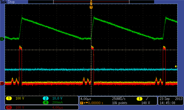
Figure 2: HV Buck in CCM with L1 = 3,3 mH. VIN = 230VRMS, VOUT = 12V, IO = 150 mA
Ch.1 (Yellow) = Switching Node, Ch.2 (Blue) = VOUT Ch.M (Red) = ΔvL1, Ch.4 (Green) = IL1
Figure 3: HV Buck in DCM with L1 = 470 μH. VIN = 230VRMS, VOUT = 12V, IO = 150 mA
Ch.1 (Yellow) = Switching Node, Ch.2 (Blue) = VOUT Ch.M (Red) = ΔvL1, Ch.4 (Green) = IL1
Figure 1b shows an alternate buck topology where the control switch is ground referenced, or “in the low side”. In general this topology is easier to implement due to the ease of driving a ground-referenced NMOSFET switch. The same combined control + HV MOSFET ICs can be used, with some capable of operating directly from the 400 VDC input and others requiring a low voltage supply for their control sections that is typically 12 VDC to 24 VDC and is generated with a discrete linear regulator. This topology is a “negative buck” when used to step a negative input voltage down to a negative voltage of lower absolute value, but when connected to a positive input voltage as shown in Figure 1b it is called the “floating buck”, “low-side buck”, or “input referenced buck” owing to the fact that the output voltage is controlled with respect to the positive input rail. The two main uses for this topology are as current sources for LED drivers and as voltage regulators for low power systems where no other circuitry requires a reference to ground on the primary. A small, AC mains-powered communications device is a good example, where the microcontroller and an isolated Interface circuit would both be powered from the voltage labeled “VLED” in Figure 1b. Figure 1c shows a buckboost regulator developing a negative output voltage referenced to the negative input rail. Typical applications for such a topology include negative voltages for powering op-amps and also for controlling TRIACs that switch AC mains in and out of circuits on the primary. Two details that require attention in buck-boost circuits are: the additional voltage stress across the MOSFET, output diode and the inductor, equal to VINPK + |VO| and also the discontinuous, high-RMS current seen by the output capacitor, similar to that of the output in a flyback converter.
3. Creepage and Clearance in Non-Isolated Applications
Safety standards such as IEC-60950 are relatively clear in stating the distance through air (clearance) and distance along a surface (creepage) between isolated primary and secondary circuits, between AC mains line and neutral and between these points and protective earth. Most standards are more difficult to interpret for other voltages, such as the positive and negative outputs of a diode rectifier that form the input voltage to AC offline circuits. The isolation category for voltage nodes within non-isolated circuits is Functional Isolation, meaning that the distance between nodes is whatever is needed for the circuits to function properly. One common way to establish guidelines for PCB layout and to evaluate the physical design of a power inductor is to review the Transient Voltage tests applied to the equipment being designed. For example, in IEC-60950 equipment operating from voltages up to 300VACrms is tested with 1500 VDC pulses if it is Class I with a protective earth ground or 2500 VDC if it is Class 2 without protective earth. 300 VACrms includes the majority of AC and HVDC applications where low power non-isolated bucks and buck-boosts are used. Arcing across PCBs can be avoided in most classes of humidity and pollution with a clearance of 1 mm per 1600 VDC. (As recommended by Underwriter´s Laboratories) Many power supply designs use the Class II ratings for creepage and clearance even if they are Class I for an added margin of safety, hence to avoid arcing during the transient voltage tests of 2500 VDC a distance between pads/terminals of the inductor used should be approximately 1,6 mm or more. In each of the three topologies of Figure 1 one side of the inductor is held to a fixed voltage and the other side is commonly referred to as the “switching node” because its voltage slews back and forth from zero to VIN (for the buck and floating buck) and from zero to (VIN + |VO|) for the buckboost. Maintaining a distance of 1,6 mm from the switching node to the other nodes in the circuit is beneficial not only for prevent arcs during transient tests, but also reduces capacitive coupling and is particularly helpful in reducing common mode noise if any traces or planes with earth ground are present on the PCB.
Figure 4: Pad-to-pad and wire-to-wire clearance in the WE-PD2 HV, WE-PD HV and WE-TI HV families
Figure 4 shows the smallest member of each of the three families of HV-rated power inductors, and shows that each more than enough clearance between the electrical connections to prevent arcing at 2500 VDC. The magnetic cores of inductors (and transformers) are considered to be conductive parts as per IEC-60950, and as such their level of insulation is functional.
4. The Danger of Using Standard Inductors
It is common practice to use the same families of through-hole and surface mount power inductors as both the energy storage elements in low voltage (< 60 VDC) DC-DC applications and for input or output filtering in offline applications. One important factor in both these applications that is often overlooked is the voltage rating of the inductors. In fact, the vast majority of power inductors lack voltage ratings in their datasheets. Good quality manufacturers can provide this information upon request, or provide information on the thickness of the varnish used or other details of the mechanical construction, but the time required to then calculate the voltage that a given inductor can withstand is completely out of step with today´s fast-paced design cycles.
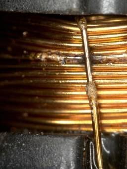 |  | 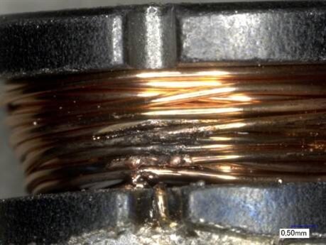 |
Figure 5: Arcing and short circuits due to overvoltage on a standard power inductor | ||
In a rush to complete design work on-time it can be tempting to select standard power inductors, but Figure 5 shows the unfortunate results that can occur when using these parts in high voltage applications – breakdown of the insulating varnish, short circuits between adjacent windings – in short, failure of a component that is normally the most robust part of a switching converter. A shorted inductor, especially one that can short AC line and neutral together during part of the switching cycle presents a genuine safety hazard to operators and service personnel. If electric shock, injury or even death occur as a result the equipment manufacturer can be held liable.
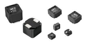
The following families of inductors are guaranteed to operate properly with up to 400 VDC according to Würth Elektronik eiSos-Standard 1516: WE-PD HV, WE-PD2 HV and WE-TI HV. Furthermore, this guarantee remains valid even after three reflow processes, making Würth Elektronik eiSos the first manufacturer in the world to provide such a robust guarantee.
5. Design Examples for Continuous Conduction Mode (CCM)
Operating in CCM, where inductor current stays above zero over the complete switching cycle, has the advantage of lower RMS currents not only in the inductor but in every other power train component as well. Lower RMS currents mean less power dissipation, lower operating temperatures, and lower electromagnetic interference (EMI). The major disadvantage is the high inductance needed, which in turn leads to physically larger inductors and sometimes to values that don´t exist as catalog products. These design examples meet the following conditions, and use the ViPER16L IC from ST Microelectronics:
| Buck And Floating Buck | Buckboost |
|---|---|
| VIN = 360 V to 400 V | VIN = 360 V to 400 V |
| VOUT = 12,0 V, ΔvO = 120 mVP-P | VOUT = -12,0 V, ΔvO = 120 mVP-P |
| IO-MAX = 200 mA, continuous | IO-MAX = 200 mA, continuous |
| Switching Frequency, fSW = 60 kHz | Switching Frequency, fSW = 60 kHz |
| POUT = 2,4 W | POUT = 2,4 W |
5.1. The Inductor
Magnetics form the heart of any switching converter, from this example delivering 2,4 W to a multiphase fullbridge converter delivering kilowatts of power. Regardless of topology, the most common way of selecting the required inductance in CCM is to specify a ripple current through the inductor, ΔiL as a percentage of the maximum average inductor current, IL-MAX. Setting ΔiL equal to 20 % to 40 % of IL-MAX represents a good compromise, tested and confirmed by the design of countless switching converters, and gives a balance between size (larger ripple requires less inductance and therefore smaller inductors) and efficiency/noise (smaller ripple leads to lower RMS currents and lower EMI).
For buck converters IL-MAX = IO-MAX, with the floating buck sharing the exact same design equations with the standard buck. In buckboost converters average inductor current is a function of duty cycle and output current. The first-order equations are for a ripple ratio of 30 % are:
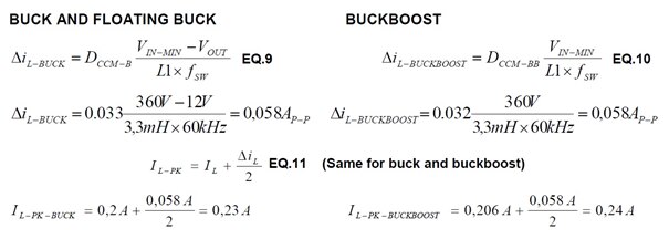
The next highest E12 value is 3,3 mH, designated L1. Once this value has been selected the actual inductor ripple current and then the peak inductor current (IL-PK) can be calculated:
With inductance average current and peak current all calculated actual inductors can be selected from the Würth Elektronik eiSos catalog. For this example the 76877093327687709332 of the WE-PD HV product family is a 3,3 mH shielded device specially designed for 400 VDC operation with an RMS current rating of 0,37 A and a peak current rating of 0,52 A. This part uses surface mount technology and is best suited to two-sided PCBs that already incorporate other SMD circuitry. Lower cost applications often use single-sided PCBs and purely through-hole technology, but in this case the principal disadvantage of CCM operation becomes plain – no 3,3 mH, HV rated through-hole parts are available.
5.2. CCM-DCM Boundary
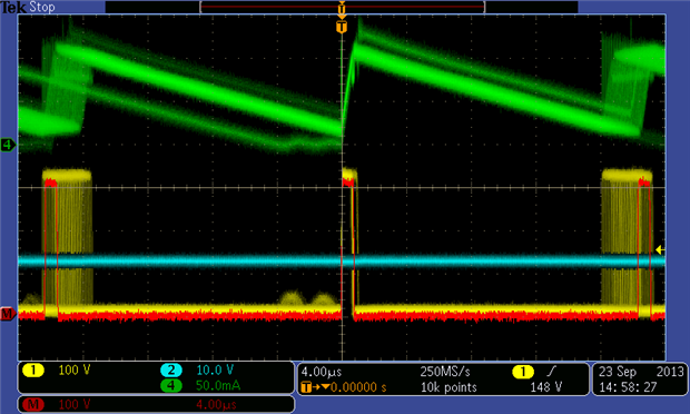
The previous example circuits can be still be operated in CCM with lower values of inductance The 768772 WE-TI HV family offers a 2,2 mH part 768772222768772222 that is rated for 0,32 A average and also 0,32 A peak that will work perfectly albeit with higher peak-to-peak ripple current The actual boundary where CCM operation is no longer possible occurs when the peak-to-peak ripple current equals exactly twice the average inductor current as illustrated in Figure 6 Note that a combination of switching frequency jitter and the input voltage ripple make it difficult to capture the inductor current touching zero hence this circuit moves back and forth across the DCM-CCM boundary from cycle to cycle
Figure 6: HV Buck on CCM-DCM boundary with L1 = 2,2 mH. VIN = 230VRMS, VOUT = 12V, IO = 57 mA
Ch.1 (Yellow) = Switching Node, Ch.2 (Blue) = VOUT Ch.M (Red) = ΔvL1, Ch.4 (Green) = IL1
The point where inductor current just reaches zero at the end of each switching cycle is often called Boundary Conduction, or BCM, and can be defined mathematically as follows:
These equations show the inductance values above which the converters would operate in CCM when delivering their maximum rated load currents. In non-synchronous converters there will always be a threshold of output current below which the converter will transition from CCM to DCM regardless of how large the inductance is. There is no harm in DCM – in fact for high voltage non-isolated applications it is actually more common to operate in DCM under the full range of load. In CCM converters, once the actual inductance has been selected the equations EQ.12 and EQ.13 can be re-written to show the threshold for boundary conduction as a function of load current. Taking the example of a 2,2 mH inductor, these would then be:
6. Design Example for Discontinuous Conduction Mode (DCM)
In DCM the current in the energy storage inductor falls to zero before the end of every switching cycle, and in order to operate in DCM the switching converter must either use a diode as the uncontrolled switch or actively control the synchronous MOSFET to prevent current from flowing backwards (from drain to source). For cost purposes it is far more common to use a diode, and for operating voltages above 200 VDC the preferred technology is the ultra-fast PN rectifier.
The principal advantage of DCM is that the inductance must be lower to ensure that the converter stays in DCM even at the highest load. Lower inductance translates to a smaller core and hence smaller, lower cost inductors. A second advantage of DCM is the reduced switching losses in the control FET, since the current in the inductor is always zero when it turns on.
Design examples for a buck/floating buck and for a buck-boost regulator operating in DCM are given below for the same set of operating conditions as the CCM example in the previous section.
6.1. Inductor Selection
The same equations used for identifying the boundary between DCM operating and CCM operation are used to select inductance for the DCM case, the only difference is that they now set a maximum permissible inductance. Repeating the results from EQ.14 and EQ.15:
In theory any value below LMAX will work, but because inductance and peak current are inversely proportional in practice it is best to select the next lowest standard value in order to prevent peak current from reaching excessive values. A standard E12 value of 470 μH will work well for both designs, and in order to select an actual device from a catalog the peak currents for each topology must be calculated. Peak current and peakto-peak ripple current are equal in DCM, and to calculate this value the duty cycle must be calculated first. With the actual inductor value selected the amount of energy transferred from input to output during each switching cycle is known, and the duty cycle of the control FET in each topology can be calculated:
The next step is to calculate the peak inductor currents:
Based upon the limits for inductance and peak current an actual inductor can be selected The 76877144717687714471 from the WE-PD HV product family is a 470 H inductor with a saturation current limit of 0,8 A
This is a surface mount part that includes magnetic shielding for low EMI and measures 10 mm x 10 mm by 6 mm tall Most important of all the 768771 family features design and post-production testing to ensure that its parts function correctly with differential voltages of up to 400 VDC Such a part would be a good choice for dualsided PCBs where an HV non-isolated buck accompanies other surface mount circuitry For simpler applications where the PCB has a single layer and less expensive through-hole parts are used for the capacitors diode MOSFET and resistors a better choice would be the 768772471768772471 from the WE-TI HV product family a through-hole device also 470 H and with a saturation current rating of 0,9 A
7. Appendix
7.1. Complete Circuit Schematic for Buck Regulator
7.2. Würth Elektronik eiSos’ High Voltage Power Inductors
The following families of inductors are guaranteed to operate properly with up to 400 VDC according to Würth Elektronik eiSos-Standard 1516, even after three reflow processes:
IMPORTANT NOTICE
The Application Note is based on our knowledge and experience of typical requirements concerning these areas. It serves as general guidance and should not be construed as a commitment for the suitability for customer applications by Würth Elektronik eiSos GmbH & Co. KG. The information in the Application Note is subject to change without notice. This document and parts thereof must not be reproduced or copied without written permission, and contents thereof must not be imparted to a third party nor be used for any unauthorized purpose. Würth Elektronik eiSos GmbH & Co. KG and its subsidiaries and affiliates (WE) are not liable for application assistance of any kind. Customers may use WE’s assistance and product recommendations for their applications and design. The responsibility for the applicability and use of WE Products in a particular customer design is always solely within the authority of the customer. Due to this fact it is up to the customer to evaluate and investigate, where appropriate, and decide whether the device with the specific product characteristics described in the product specification is valid and suitable for the respective customer application or not. The technical specifications are stated in the current data sheet of the products. Therefore the customers shall use the data sheets and are cautioned to verify that data sheets are current. The current data sheets can be downloadded at www.we-online.com. Customers shall strictly observe any product-specific notes, cautions and warnings. WE reserves the right to make corrections, modifications,enhancements, improvements, and other changes to its products and services.
WE DOES NOT WARRANT OR REPRESENT THAT ANY LICENSE, EITHER EXPRESS OR IMPLIED, IS GRANTED UNDER ANY PATENT RIGHT, COPYRIGHT, MASK WORK RIGHT, OR OTHER INTELLECTUAL PROPERTY RIGHT RELATING TO ANY COMBINATION, MACHINE, OR PROCESS IN WHICH WE PRODUCTS OR SERVICES ARE USED. INFORMATION PUBLISHED BY WE REGARDING THIRD-PARTY PRODUCTS OR SERVICES DOES NOT CONSTITUTE A LICENSE FROM WE TO USE SUCH PRODUCTS OR SERVICES OR A WARRANTY OR ENDORSEMENT THEREOF.
WE products are not authorized for use in safety-critical applications, or where a failure of the product is reasonably expected to cause severe personal injury or death. Moreover, WE products are neither designed nor intended for use in areas such as military, aerospace, aviation, nuclear control, submarine, transportation (automotive control, train control, ship control), transportation signal, disaster prevention, medical, public information network etc. Customers shall inform WE about the intent of such usage before design-in stage. In certain customer applications requiring a very high level of safety and in which the malfunction or failure of an electronic component could endanger human life or health, customers must ensure that they have all necessary expertise in the safety and regulatory ramifications of their applications. Customers acknowledge and agree that they are solely responsible for all legal, regulatory and safety-related requirements concerning their products and any use of WE products in such safety-critical applications, notwithstanding any applications-related information or support that may be provided by WE. CUSTOMERS SHALL INDEMNIFY WE AGAINST ANY DAMAGES ARISING OUT OF THE USE OF WE PRODUCTS IN SUCH SAFETY-CRITICAL APPLICATIONS.
USEFUL LINKS
Application Notes: http://www.we-online.com/app-notes
REDEXPERT Design Tool: http://www.we-online.com/redexpert
Toolbox: http://www.we-online.com/toolbox
Product Catalog: http://katalog.we-online.de/en/
DIRECT LINK
ANP021: Safe, Reliable Designs for Non-Isolated Offline Switchers with 400VDC Rated Power Inductors
CONTACT INFORMATION
Würth Elektronik eiSos GmbH & Co. KG
Max-Eyth-Str. 1, 74638 Waldenburg, Germany
Tel.: +49 (0) 7942 / 945 – 0
Email: appnotes@we-online.de


