element14 Community
element14 Community
    Register Log In
  • Site
  • Search
  • Log In Register
  • About Us
  • Community Hub
    Community Hub
    • What's New on element14
    • Feedback and Support
    • Benefits of Membership
    • Personal Blogs
    • Members Area
    • Achievement Levels
  • Learn
    Learn
    • Ask an Expert
    • eBooks
    • element14 presents
    • Learning Center
    • Tech Spotlight
    • STEM Academy
    • Webinars, Training and Events
    • Learning Groups
  • Technologies
    Technologies
    • 3D Printing
    • FPGA
    • Industrial Automation
    • Internet of Things
    • Power & Energy
    • Sensors
    • Technology Groups
  • Challenges & Projects
    Challenges & Projects
    • Design Challenges
    • element14 presents Projects
    • Project14
    • Arduino Projects
    • Raspberry Pi Projects
    • Project Groups
  • Products
    Products
    • Arduino
    • Avnet Boards Community
    • Dev Tools
    • Manufacturers
    • Multicomp Pro
    • Product Groups
    • Raspberry Pi
    • RoadTests & Reviews
  • Store
    Store
    • Visit Your Store
    • Choose another store...
      • Europe
      •  Austria (German)
      •  Belgium (Dutch, French)
      •  Bulgaria (Bulgarian)
      •  Czech Republic (Czech)
      •  Denmark (Danish)
      •  Estonia (Estonian)
      •  Finland (Finnish)
      •  France (French)
      •  Germany (German)
      •  Hungary (Hungarian)
      •  Ireland
      •  Israel
      •  Italy (Italian)
      •  Latvia (Latvian)
      •  
      •  Lithuania (Lithuanian)
      •  Netherlands (Dutch)
      •  Norway (Norwegian)
      •  Poland (Polish)
      •  Portugal (Portuguese)
      •  Romania (Romanian)
      •  Russia (Russian)
      •  Slovakia (Slovak)
      •  Slovenia (Slovenian)
      •  Spain (Spanish)
      •  Sweden (Swedish)
      •  Switzerland(German, French)
      •  Turkey (Turkish)
      •  United Kingdom
      • Asia Pacific
      •  Australia
      •  China
      •  Hong Kong
      •  India
      •  Korea (Korean)
      •  Malaysia
      •  New Zealand
      •  Philippines
      •  Singapore
      •  Taiwan
      •  Thailand (Thai)
      • Americas
      •  Brazil (Portuguese)
      •  Canada
      •  Mexico (Spanish)
      •  United States
      Can't find the country/region you're looking for? Visit our export site or find a local distributor.
  • Translate
  • Profile
  • Settings
PCB Design, Prototyping and Production
  • Products
  • More
PCB Design, Prototyping and Production
PCB Forum PCB Design for a DC Load Part 2
  • Blog
  • Forum
  • Documents
  • Leaderboard
  • Files
  • Members
  • Mentions
  • Sub-Groups
  • Tags
  • More
  • Cancel
  • New
Join PCB Design, Prototyping and Production to participate - click to join for free!
Actions
  • Share
  • More
  • Cancel
Forum Thread Details
  • Replies 12 replies
  • Subscribers 129 subscribers
  • Views 2757 views
  • Users 0 members are here
Related

PCB Design for a DC Load Part 2

Andrew J
Andrew J over 3 years ago

Given the way the forum software works, I've started a new discussion on this topic so that it might get some visibility; unfortunately, responding to the original wouldn't pop it to the front as recent content and it appears I can't change the publish date of a forum posting which makes sense.  Anyway, I made the first post on the subject a while ago here and if you haven't read it yet, the following may make no sense as it is a carry on.

I was fortunate that ScottieBabe spotted the 0.5mm thermal relief on the current sensor connector because I'd missed it.  This was of course deliberate to see if anyone was paying attention.  Not.  I thought I could patch that up but looking closely I’d made a big error on the connector footprints: one of the pins had no direct connection to the fill zone (electrically, not a problem because the two pins are connected) and the second pin only had 0.5mm thermal reliefs.  This wasn’t obvious to me because of the zone fills but extra eyes spotted it, now it's blatantly obvious and I can’t realistically patch them all so I’m making a new board.  

The issue arose because of how Kicad handles footprints and how I’d found out how to create footprints that overlapped - custom shapes.  With a custom shape there are two options for connecting: NONE and SOLID; this is different to ‘normal’ footprints which have the additional options of PARENT FOOTPRINT and THERMAL RELIEF.  This makes sense as how would Kicad know how to create thermal reliefs for a custom shape?  As I hadn’t realised, one pad (the custom one) was set to NONE and the other to PARENT - that parent was the fill zone which had a thermal relief setting of 0.5mm.  Turns out I didn’t need to create the overlapping pad as a custom shape, but could set it to be rectangular, 1mm larger than it needed to be and offset in the X-axis by 1mm.  This allowed it to overlap but still be within the dimension of the pad at the bottom of the connector.  Lesson learned (and a top tip for Kicad there.  You’re welcome.)

Updated Board

Front Side, Bcu hidden: 

Front Side of DC Load PCB

Back side, Fcu hidden:

Back Side of DC Load PCB

What I have done

I took the opportunity to make some more changes as well, based on feedback:

  • Moved the DRAIN fill zone to the bottom of the board and made it much larger.
  • Increased the size of the SOURCE zones and ensured they are the same size across all MOSFETs.
  • Increased the size of the high current path to the sense resistor.
  • Changed the connector footprints to use 3mm thermal reliefs with 0.5 mm thermal relief gap.  According to Kicad’s calculator, a 2.8mm wide, 0.5mm long track would drop 450uV for a 10C rise at 5A.

This keeps the parts the same which I hope to salvage from the old board.   I can also reuse the stencil I had created.

What I could do

Jon mentioned using Thick Film resistors instead of the wire wounds I have because they have lower inductance - in fact, looking at data sheets, it would seem to be negligible inductance.  This doesn’t seem to be a parameter reported on wire wound resistors so I can’t compare.  I could use this 1Ohm Thick Film resistor , which has a much better temperature de-rating and coefficient, instead of the 1 Ohm wire wound resistor.   With some adjustment to the run of the -5V trace, I could get this to straddle the trace linking R20, R17, R14 and R10.  Worth it for an extra £18.50?

I did a quick check with LTSpice to double-check the power requirements of the resistors as well: approx 2W.  I’m rubbish at LTSpice though, so it could be wrong…

LT Spice schematic with run results showing power used by the 1Ohm resistors on the source of the MOSFETs at 5Amps

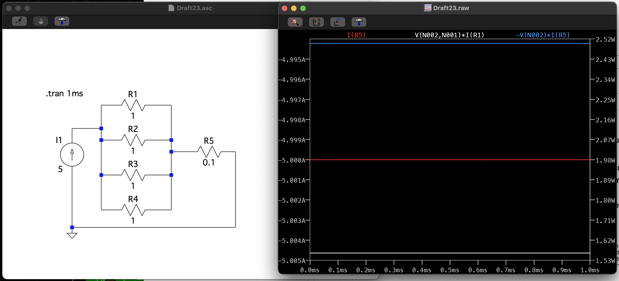
This is showing just over 1.5W at 5A.

What I struggled with

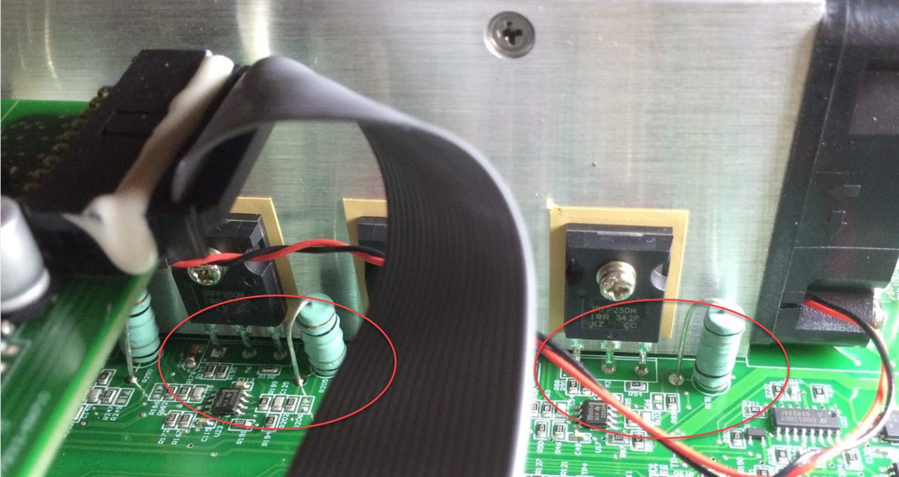
Thinking about the loop and potential induction.  I have, in total, 7 TO-220 devices to connect to the heatsink and 6 of them are directly involved in moving the load from J11 to J12 (the other is a temperature monitor.)  I really wanted to use connectors for these devices to make it easier to replace them if damaged, or remove the board from the enclosure without having to disturb them.  The alternative is to line them along the edge of the board so they can still be attached to a heatsink but that would still take 105mm vs the 174mm currently (a 70mm shorter path.)  With judicious positioning I might be able to make that difference 80-90mm, perhaps 100mm.  An extra 100mm of wire (if I didn’t do it) would introduce approximately 100nH but I don’t know if that’s a lot or not, or the impact.  That all has to be considered against the convenience of using the connectors.

What I could do - and I don’t know if this would help or not - is to replace the J11 and J12 connectors with single M3 holes into which I could screw the Load leads.  The replacement J12 hole, I could move next to the J11 hole and run the +5Vgnd (sorry ScottieBabe!) across the back of the board on a, say, 10 mm track from the sense resistor (for the purpose of inductance, I don’t think width matters actually.)  This would entail making the board a bit wider but apart from a small-ish cost, isn’t an issue for the enclosure  However, really, the overall loop is still the same whether completed by a wire or a trace so I don’t know if that would be of great benefit?  

Ultimately, I couldn’t work out an alternative placement option for the MOSFETs that kept them on the heatsink AND reduced the inductance loop significantly.   Also, that kept the mounting at least reasonably convenient.


As I'm having the board remade, now is the opportunity to make any further adjustments that may be worth it.

  • Sign in to reply
  • Cancel

Top Replies

  • jc2048
    jc2048 over 3 years ago +6
    "What I struggled with" I'm not sure how helpful my previous comments on the other thread were. Leaving aside the wirewound resistors (properties unknown), I think probably what is the most significant…
  • jc2048
    jc2048 over 3 years ago in reply to Andrew J +5
    How odd. Somehow, I totally missed seeing the white line. Not sure how I did that - probably, it was your "approx 2W" steering me to the wrong lines. Sorry about that (I blame it on old age!) I still…
  • Andrew J
    Andrew J over 3 years ago in reply to jc2048 +4
    Thanks John - I'm going to see what happens when I hook it all up. I can already see some worthwhile changes from the comments so even this board will go through a revision, and I may as well wait now…
  • jc2048
    jc2048 over 3 years ago

    Re: the 1R sharing resistors

    For 5A, each resistor handles a quarter of that: approx 1.25A. Power is I^2 x R, so about 1.56W with a 1R resistor. (Your simulation is giving you the dissipation of the 0.1R sense resistor.)

    These parts in the following link can manage 2W, but will be running hot on 1.25A and it might be problematic, depending on how high the ambient in your enclosure gets.

    https://uk.farnell.com/panasonic/erjc1bf1r0u/current-sense-res-1r-1-2-w-2010/dp/2353353

    To get the dissipation in each device down, you could place two in parallel to give 0.5R in series with another pair to bring it up to 1R again. That would then quarter the dissipation in each resistor, but then the cost is getting towards what you'd pay with the one you've found (though it would make for a neater build on the board).

    They'd certainly be very low in inductance (little more than an equivalent width of pcb trace).

    I've got no feel at all as to how troublesome the inductance of the wirewound resistors might be, but the MOSFET has gain up to the tens of megahertz area and there is (intrinsic) capacitance in the device to react with the inductance, so it's something to be a little wary of. Are you going to try the pcb you've had made and find out?

    • Cancel
    • Vote Up +3 Vote Down
    • Sign in to reply
    • Cancel
  • Andrew J
    Andrew J over 3 years ago in reply to jc2048

    The simulation shows both Jon, with the 1Ohms at the bottom around the 1.56W mark.  I’m not sure why I wrote 2W above the image and 1.5W underneath it: excessive rounding I think.  Those parts you linked to are about half the price of the one I did, but there were cheaper ones - mainly it was the footprint that allowed me to straddle the trace!  I vacillate on using the board I have because all the high current parts are connected through 0.5mm thermal relief traces and I should just bite the bullet; on the other hand I can check the circuit works and make further adjustments.  It obviously makes sense, but plenty of time yet as I’m very slow on developing the control side.

    • Cancel
    • Vote Up +2 Vote Down
    • Sign in to reply
    • Cancel
  • jc2048
    jc2048 over 3 years ago in reply to Andrew J

    How odd. Somehow, I totally missed seeing the white line. Not sure how I did that - probably, it was your "approx 2W" steering me to the wrong lines. Sorry about that (I blame it on old age!)

    I still think my InHead simulator is quicker; though I would have guessed an approximate 1.6 for the square of 1.25 rather than bother to calculate it properly.

    Are the thermal reliefs on the existing board much of a problem? They're very short, so the temperature rise of the track is nothing like you'd get with a long trace (the large areas of trace copper next to them and the component lead metal both act to heatsink them). They'll carry far more current than the figure for a similar width of track would suggest. The only point where the small additional resistance is of consequence is at the sense resistor, but you're going to have to adapt that area anyway to improve what you've done with the sense (one way to do that, quickly, to get your prototype going, would be to swerve round the tracking problem entirely and run a twisted pair of sense lines back to where you need them, directly from the sense resistor terminals).

    • Cancel
    • Vote Up +5 Vote Down
    • Sign in to reply
    • Cancel
  • shabaz
    shabaz over 3 years ago

    Hi Andrew,

    Nice looking board! I don't know what connectors you're planning to use, another (maybe unorthodox) option could be to surface-mount the through-hole MOSFETs, i.e. have rectangular long pads (they could have several vias in them for connecting to the other side, and giving strength to the pad) for the MOSFET legs, and that way you still retain the benefit of easily being able to lift off a MOSFET. It will be quicker than soldering wires to the MOSFETs, but does entail more accurate drilling. 

    That will just make it quicker to assemble, not really any other technical reason. Anyway it's just an idea. Maybe not worth doing now that the design is nicely laid out with the connectors.

    Also, since the transistor traces are all on one side, maybe it could be convenient to replace with (say) BC847 etc., probably easier to solder. This too is minor, probably not worth it unless other changes were being made.

    • Cancel
    • Vote Up +3 Vote Down
    • Sign in to reply
    • Cancel
  • Andrew J
    Andrew J over 3 years ago in reply to jc2048

    I will give it a go for sure, TBH, there's no real compelling reason not to. The wires are a good idea but in reality I already have that wide trace in place so it's just the narrow trace to the sense resistor connector.  Anyway, I guess try it and see.

    • Cancel
    • Vote Up +2 Vote Down
    • Sign in to reply
    • Cancel
  • Andrew J
    Andrew J over 3 years ago in reply to shabaz

    Thanks Shabaz.  I put a link to the connectors (and picture of the populated board) in the first post, linked above.  They're just single pole, 2 pin, lever connectors for convenience and I think I'll stick with them until/if they prove an issue.  I'd considered a number of options in terms to the TO-220 mounting including as you say soldering the legs to the bottom of the board and having the heatsink underneath.  I'd also considered changing those 2N2222 components, seeing as I was changing the board, but I've got about 20 of them and they're not getting used up so I'm going to stick with them.  I think what I really wanted to avoid was disturbing the layout of the surface mount parts as that was a challenge to lay them out in such a way as to stick with a two-layer board.  At the size it is, 4-layer is quite expensive.

    • Cancel
    • Vote Up +3 Vote Down
    • Sign in to reply
    • Cancel
  • jc2048
    jc2048 over 3 years ago

    "What I struggled with"

    I'm not sure how helpful my previous comments on the other thread were.

    Leaving aside the wirewound resistors (properties unknown), I think probably what is the most significant inductance in the output loop is what the user adds with the test leads connecting it to the circuit under test, and the properties of the circuit being tested itself. You have to live with that and just take precautions to protect your load where possible.

    The stubs out to the MOSFETs don't need to add much in the way of inductance. Your figure is for the wire self-inductance. That assumes that there is nothing nearby to influence things (ie the wire is long and the return is not nearby). In practice, if you run the drain wire alongside the source wire, there will be a lot of field cancellation between the magnetic fields generated by each. For the stub, you'll have almost a complete single turn, but with next to no loop cross-sectional area, so hence a low inductance for the partial turn.

    It should be ok. Just try it and see how you get on. The currents you're working with here are quite modest.

    A more glaring problem, and the one you might want to think about a bit more, is two lots of contact resistance adding to the resistance of the sense resistor [you are measuring the voltage on the board side of the connection]. If your sense resistor is 100mR, then the contact resistance could add a few % to that. As you develop the board, the contact resistance will change somewhat as you use the connectors. Are you going to live with any inaccuracy? Are you going to calibrate the unit? How will you deal with it changing if you want to take the whole thing apart later and put it back together again?

    The other question with the sense is obviously the temperature dependence. Something like 200ppm might not sound too bad, but it's 0.5% with only a 25C rise. I take it you're dealing with that in part by heatsinking, to reduce the effect of the self-heating, but are you also measuring the temperature, or will it be accurate enough for what you want without any correction?

    I agree with what Scottie said about the op-amp decoupling ground and about having a Kelvin connection to the sense.

    "for the purpose of inductance, I don’t think width matters actually."

    I think you'll find a wider trace has lower self-inductance than a narrow trace (for the same weight of copper, obviously). I can certainly convince myself of that with a simple thought experiment, though I might well be wrong (I never did pay attention properly when doing the Electricity & Magnetism stuff at school and still fail to remember when you apply the 'righthand rule' and when the left, and which finger represents which quantity - amazing I managed to design things, really).

    • Cancel
    • Vote Up +6 Vote Down
    • Sign in to reply
    • Cancel
  • Andrew J
    Andrew J over 3 years ago in reply to jc2048

    Thanks John - I'm going to see what happens when I hook it all up.  I can already see some worthwhile changes from the comments so even this board will go through a revision, and I may as well wait now to see what else might be useful!  

    I'm mulling over the repositioning of the LOAD + and LOAD - connectors to be together, and re-ordering the TO-220s on the board so I can better position the current sense resistor for kelvin connection to the ADC (off board): I need to look at that more closely actually, as the ADC is wired up as single ended inputs.  

    It may also be worth looking at this SMD resistor which is rated for 10W with a temp coefficient of 75ppm/C (possibly down towards 25ppm/C with the sense connections) compared to the 100ppm/C with the TO-220 one I have at the moment.  The max power through the sense resistor is 2.5W (I'm sort of basing this on 5A but I really don't think I'm looking at any more than 3A / 0.9W in practice as the MOSFETs and heat sinking available is going to limit things) but it doesn't give any thermal information, except a de-rating chart, so I can't tell what temperature rise it's going to undergo.  Also, the heating impact on the rest of the board.  I need to think about that a bit more too.

    I do have heatsinking and a temperature monitor - in fact a temperature monitor and two thermistors - with some capability to do some on-board adjustment as well as, potentially, some software adjustment.  I put in two because I had spare ADC inputs (so why not??) and I thought it may be useful for characterising the temperature rises of the MOSFETs when I was testing.  I could repurpose one of those to use as an additional sense input and ultimately use one as an ambient temperature sensor.  All just ideas at the moment!

    I'm not sure what you mean by op-amp decoupling - I have decoupling capacitors on both my ICs.  I think ScottieBabe mentioned it would be a good idea to put in a pull-down resistor on the multiplexor output to ensure signal state to the op-amp when the multiplexor is off.  That's a good idea and I'm going to test the output signal before shuffling components around to fit it.

    • Cancel
    • Vote Up +4 Vote Down
    • Sign in to reply
    • Cancel
  • jc2048
    jc2048 over 3 years ago in reply to Andrew J

    Yes, there's a bit of a trade off with the sense resistors. If the one in a big package on a heatsink rises much less in temperature as a consequence, then the change in resistance for a given current might be similar, even though on paper, from the temperature coefficients, it might initially look like a worse choice.

    If the power in the sense resistor is getting difficult, you could consider dropping the resistance value.

    The decoupling of the op amp is needed between the positive and negative supply terminals (the device doesn't normally have a GND connection). It can be done with a single capacitor. Often people use two capacitors, with the reference ground acting as a intermediary between the two capacitors. As long as the join between the two is very short and fat, that's almost as good as a single capacitor. But in your case you have two grounds, with the join off on another board, and two lots of resistance and inductance added into the circuit. You're building a very imperfect capacitor. Does it matter? Possibly not: it's only to improve the high-frequency PSRR.

    • Cancel
    • Vote Up +3 Vote Down
    • Sign in to reply
    • Cancel
  • shabaz
    shabaz over 3 years ago

    There's some interesting photos of a BK Precision electronic load here (snippet of one of the photos is below), it looks like they tried to solve the load sharing problem by having a separate op amp per MOSFET. It's more expensive, but might be worth considering or ruling out. It does make things easier in that it shifts the requirement to just needing accurately matched resistors, which is easy to do. 

    image

    There is also discussion here: https://www.eevblog.com/forum/projects/dynamic-electronic-load-project/msg288313/#msg288313 where two different model MOSFETs were attempted, and the op-amp and resistors resolved it to do the load-sharing. Maybe this is too large a change if what you already have works, but I thought I'd mention it in case it helps.

    Another slightly unorthodox thing, could be to buy manganin wire (it's available from wires.co.uk), and they have 0.45mm diameter wire (for instance), which equals 0.1 ohm with a length of 36.99 mm, which would have very little inductance, about 20 nH, if (say) it was wound into a coil of 6mm diameter, which would be 2 turns (or there are ways to wind with lower inductance, but maybe that's not needed since it is just 2 turns). It is very stable over temperature, a bit pricey for a reel of it, but overall low-cost since it could make hundreds of resistors, and the same footprint could be used for a normal resistor. It solders fine, like normal wire. If you would like some to experiment with, let me know, since I have a reel of 0.45mm diameter, and I'd be happy to post some (I'm very unlikely to use it all).

    • Cancel
    • Vote Up +2 Vote Down
    • Sign in to reply
    • Cancel
>
element14 Community

element14 is the first online community specifically for engineers. Connect with your peers and get expert answers to your questions.

  • Members
  • Learn
  • Technologies
  • Challenges & Projects
  • Products
  • Store
  • About Us
  • Feedback & Support
  • FAQs
  • Terms of Use
  • Privacy Policy
  • Legal and Copyright Notices
  • Sitemap
  • Cookies

An Avnet Company © 2025 Premier Farnell Limited. All Rights Reserved.

Premier Farnell Ltd, registered in England and Wales (no 00876412), registered office: Farnell House, Forge Lane, Leeds LS12 2NE.

ICP 备案号 10220084.

Follow element14

  • X
  • Facebook
  • linkedin
  • YouTube