element14 Community
element14 Community
    Register Log In
  • Site
  • Search
  • Log In Register
  • About Us
  • Community Hub
    Community Hub
    • What's New on element14
    • Feedback and Support
    • Benefits of Membership
    • Personal Blogs
    • Members Area
    • Achievement Levels
  • Learn
    Learn
    • Ask an Expert
    • eBooks
    • element14 presents
    • Learning Center
    • Tech Spotlight
    • STEM Academy
    • Webinars, Training and Events
    • Learning Groups
  • Technologies
    Technologies
    • 3D Printing
    • FPGA
    • Industrial Automation
    • Internet of Things
    • Power & Energy
    • Sensors
    • Technology Groups
  • Challenges & Projects
    Challenges & Projects
    • Design Challenges
    • element14 presents Projects
    • Project14
    • Arduino Projects
    • Raspberry Pi Projects
    • Project Groups
  • Products
    Products
    • Arduino
    • Avnet Boards Community
    • Dev Tools
    • Manufacturers
    • Multicomp Pro
    • Product Groups
    • Raspberry Pi
    • RoadTests & Reviews
  • Store
    Store
    • Visit Your Store
    • Choose another store...
      • Europe
      •  Austria (German)
      •  Belgium (Dutch, French)
      •  Bulgaria (Bulgarian)
      •  Czech Republic (Czech)
      •  Denmark (Danish)
      •  Estonia (Estonian)
      •  Finland (Finnish)
      •  France (French)
      •  Germany (German)
      •  Hungary (Hungarian)
      •  Ireland
      •  Israel
      •  Italy (Italian)
      •  Latvia (Latvian)
      •  
      •  Lithuania (Lithuanian)
      •  Netherlands (Dutch)
      •  Norway (Norwegian)
      •  Poland (Polish)
      •  Portugal (Portuguese)
      •  Romania (Romanian)
      •  Russia (Russian)
      •  Slovakia (Slovak)
      •  Slovenia (Slovenian)
      •  Spain (Spanish)
      •  Sweden (Swedish)
      •  Switzerland(German, French)
      •  Turkey (Turkish)
      •  United Kingdom
      • Asia Pacific
      •  Australia
      •  China
      •  Hong Kong
      •  India
      •  Korea (Korean)
      •  Malaysia
      •  New Zealand
      •  Philippines
      •  Singapore
      •  Taiwan
      •  Thailand (Thai)
      • Americas
      •  Brazil (Portuguese)
      •  Canada
      •  Mexico (Spanish)
      •  United States
      Can't find the country/region you're looking for? Visit our export site or find a local distributor.
  • Translate
  • Profile
  • Settings
PCB Design, Prototyping and Production
  • Products
  • More
PCB Design, Prototyping and Production
PCB Forum Is there such a PCB construction technique?
  • Blog
  • Forum
  • Documents
  • Leaderboard
  • Files
  • Members
  • Mentions
  • Sub-Groups
  • Tags
  • More
  • Cancel
  • New
Join PCB Design, Prototyping and Production to participate - click to join for free!
Actions
  • Share
  • More
  • Cancel
Forum Thread Details
  • State Not Answered
  • Replies 13 replies
  • Subscribers 128 subscribers
  • Views 3505 views
  • Users 0 members are here
  • pcb manufacture
  • pcb prototyping
  • pcb fabricating
Related

Is there such a PCB construction technique?

colporteur
colporteur over 2 years ago

image

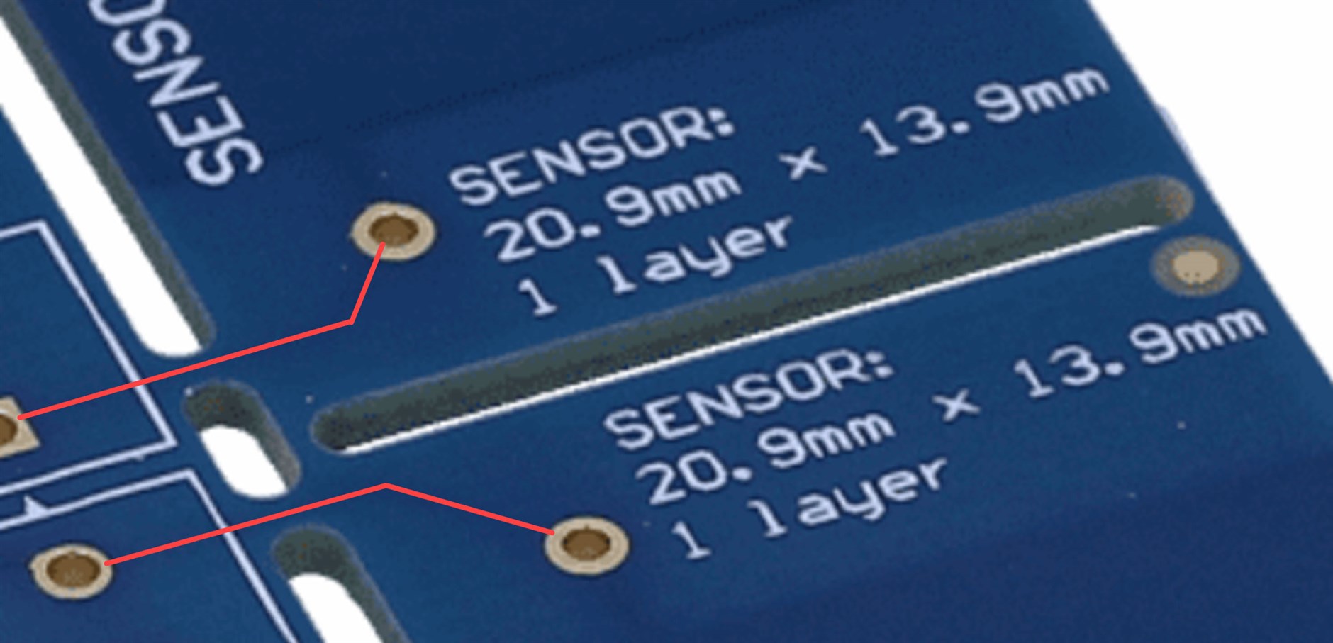
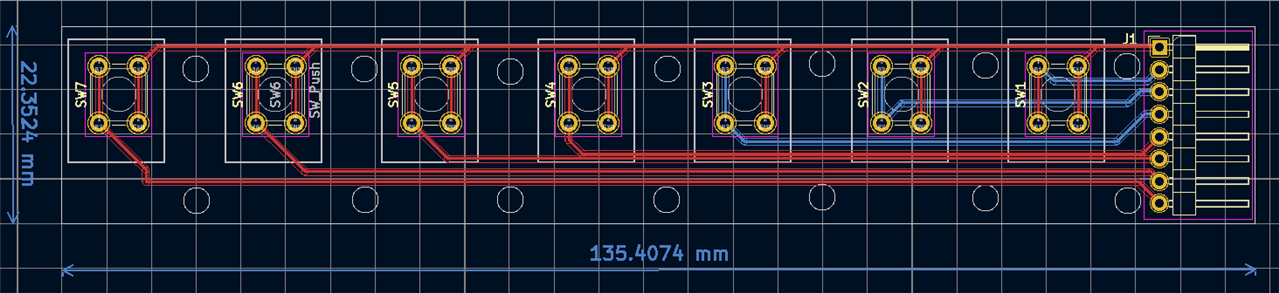
Is there a PCB construction that creates an area of the board that can easily be broken?

In the sketch the dotted section could be easily broken to reduce the size PCB. My design would have each breakout section containing a button(s) that wire back to a single edge connector. Breaking off pieces of the PCB reduces the number of buttons. 

I was wonder if such a technique is used and what it might be called when constructing a PCB?

  • Sign in to reply
  • Cancel

Top Replies

  • Gough Lui
    Gough Lui over 2 years ago +4
    Yes, there is several techniques that can be used to make divisible PCBs. One is to use V-scoring to cut a channel - this results in a cut line which can be snapped to divide the PCB but nothing can…
  • Gough Lui
    Gough Lui over 2 years ago in reply to Andrew J +2
    Andrew J said: panelling This is when you want to create multiple identical PCBs but have them all attached together as a single "large" board. This is usually done for reasons of easier automated population…
  • Andrew J
    Andrew J over 2 years ago in reply to Gough Lui +2
    If that is the case, it would be even more cost effective than to have them made individually with some form of edge connectors - e.g. as beacon-Dave mentions. It’s something crazy like $1.50 per up to…
  • Gough Lui
    0 Gough Lui over 2 years ago

    Yes, there is several techniques that can be used to make divisible PCBs.

    One is to use V-scoring to cut a channel - this results in a cut line which can be snapped to divide the PCB but nothing can be routed through the cut. Many manufacturers charge extra for V-scoring.

    Another is to use routed slots to create large rounded-rectangular slots in the board. Some manufacturers won't do this at all because of the amount of drill wear it causes, and/or they may not be able to process such boards.

    Finally, what you have illustrated is more like "stamp holes" or "mousebites" where you can divide the PCB with many small hole drills. This is sometimes combined with slots as above to create divisble PCBs, sometimes with wiring between sections that can be broken-off. Some PCB manufacturers charge extra for this service as it can create multiple PCB designs, others due to excessive number of holes.

    - Gough

    • Cancel
    • Vote Up +4 Vote Down
    • Sign in to reply
    • Verify Answer
    • Cancel
  • Andrew J
    0 Andrew J over 2 years ago

    Isn’t this what PCB manufacturers called panelling?  You can set up panels of the PCB design and the v-cuts are added during manufacture.  If the boards are all different then it isn’t of course!   It those are your Google terms: panels, v cuts, and mouse bites.  Additionally, if the boards are all the same, JLCPCB will create 5 of them for the price of one in any case (I received 6 boards last time actually) so separating them isn’t necessary.  If they are all different, their price is so cheap for 2-layer boards, it’s easy enough to have them manufacturer them individually and ship them together in one order.

    I seem to recall Shabaz posting something not too long ago showing a design that required breaking the board.  You could perhaps attempt the near impossible and try and find it!

    • Cancel
    • Vote Up +1 Vote Down
    • Sign in to reply
    • Verify Answer
    • Cancel
  • Gough Lui
    0 Gough Lui over 2 years ago in reply to Andrew J
    Andrew J said:
    panelling

    This is when you want to create multiple identical PCBs but have them all attached together as a single "large" board. This is usually done for reasons of easier automated population and soldering by manufacturing equipment when a run of boards is required. Sometimes there are defects on these panels - depending on what option is selected and paid for, either you can get perfect panels or X-out panels where bad boards have an X marked on them. Such panelled boards can be attached by mousebites or V-scoring depending on the manufacturer, and often requires a handling zone on the edge in the form of a "rail". Often PCB manufacturing houses can help by performing the necessary data processing to create panels that their systems can handle.

    From what I gather from the question, the PCB is being made to be "adaptable" in the sense that it may be made up as eight buttons and have unneeded parts snapped off. Not exactly something I would consider a panel, but more a divisible/separable PCB, so I would expect the designer to have to put this into the design, rather than the PCB manufacturer.

    - Gough

    • Cancel
    • Vote Up +2 Vote Down
    • Sign in to reply
    • Verify Answer
    • Cancel
  • beacon_dave
    0 beacon_dave over 2 years ago in reply to Gough Lui

    "...One is to use V-scoring to cut a channel - this results in a cut line which can be snapped to divide the PCB but nothing can be routed through the cut..."

    Could perhaps leave pads either side of the V-score to allow wire links to jump the groove. Perhaps space it appropriately to accommodate a pair of right-angle connectors giving the option of easily re-joining snapped sections back together again.

    • Cancel
    • Vote Up 0 Vote Down
    • Sign in to reply
    • Verify Answer
    • Cancel
  • Andrew J
    0 Andrew J over 2 years ago in reply to Gough Lui

    If that is the case, it would be even more cost effective than to have them made individually with some form of edge connectors - e.g. as beacon-Dave mentions.  It’s something crazy like $1.50 per up to 100mmx100mm board design and you get 5 of them!  That means you could end up with 5 sets to sell/give away.  

    anyway, not to derail the original question, I think your answer of v-cuts is how it is done.

    • Cancel
    • Vote Up +2 Vote Down
    • Sign in to reply
    • Verify Answer
    • Cancel
  • beacon_dave
    0 beacon_dave over 2 years ago

    If you are aiming to separate the PCB before populating it, then another option might be to get the likes of a small PCB guillotine. Mark the cutting points on the silkscreen layer for easy alignment.

    • Cancel
    • Vote Up +2 Vote Down
    • Sign in to reply
    • Verify Answer
    • Cancel
  • dougw
    0 dougw over 2 years ago

    I used to panelize cards in the artwork and cut them out after fabrication with sheet metal shears. Then I cleaned up the edges with a file. Back then they charged extra for drilling holes, v-cuts and routing slots so I didn't use those methods. Now, with individual cards at $0.50 each, I don't bother with panelizing, I just buy individual cards. 

    • Cancel
    • Vote Up +2 Vote Down
    • Sign in to reply
    • Verify Answer
    • Cancel
  • shabaz
    0 shabaz over 2 years ago

    Hi Sean,

    There are lots of options, for instance if you need enough of them, (e.g. in the tens of them), economically it may just work out that getting a load of them in different lengths is cheaper, as Andrew says, the costs are so low for a basic board, there is less reason to make them with the snap-off capability. I had a board with several different sections, but I gave up and just ordered 50 or so of each of the sections, and even if some go unused, it was still cheaper. Personally I like this option, because it's cheaper production since there are less operations, and the boards are easier to use because they do not need sanding etc after they have been snapped off (not essential, but it bothers me if I don't.

    Another option is to make the board the minimum size but easy to solder together (if you're not using the board shape for strength too), for instance for touch buttons, I went with a 2x2 array, and the boards can be fitted next to each other for (say) a 2x4 array. In that case, I used a separate cheap connector on each board though.

    Often with the drilled hole method, it can be combined with slots, i.e. the board may have slots, and then some small holes (mousebites). There will likely be examples of it online, with suggested dimensions. Some development boards do a similar thing, to (say) snap off the debugger from the rest of the board

    The guillotine idea is nice too. It will flex the board slightly, but for the size of board and the use-case, it's likely no issue. It's more effort though, compared to a load of ready-made boards of the right dimensions.

    Incidentally, for some projects, as a more far-out idea, perhaps aluminium PCBs are another option too, since they are getting to be very low-cost, e.g. if you want to make board that can be broken off by metal fatigue with a sharp bend along holes, but can also be used to take on a different shape through smaller angle bends. I experimented a little bit with aluminium PCB bends here:  XR-1000 Chassis and Electromechanicals: Putting it Together however I still need to learn more about that. One would probably need to initially experiment with a few iterations to make it a useful technique for their end application (if it is usable at all, because it has some significant limitations too). 

    Examples from an eval board (TI FDC sensor board). The left and right side pads are connected on the underside, I've drawn red lines to show the traces. They used slots to make the board easier to snap off, because the small holes on their own would be difficult to snap apart with hands.

    image (image sources: TI website)

    Here they used large slots:

    image

    • Cancel
    • Vote Up +1 Vote Down
    • Sign in to reply
    • Verify Answer
    • Cancel
  • shabaz
    0 shabaz over 2 years ago

    Also, if you don't mind ordering thinner PCBs, then it's possible to cut with some scissors, with no slots or holes necessary. You can just draw on the silkscreen layer, a line to guide the scissors visually : ) 

    This was a 0.8mm board I think, and it costs about the same (or very little extra).

    image

    The faint grid dots are 1mm spaced in the screenshot below, to get an idea of the size of the board (it is a 7mm wide strip basically). I added a few tiny holes (yellow) on the silkscreen line, but they were not necessary, but no harm to add them to make it a bit easier.

    image

    This was an LED strip board, where I just wanted a couple of different options to snip off a few LEDs. I guess a similar idea to the buttons you mention.

    • Cancel
    • Vote Up +1 Vote Down
    • Sign in to reply
    • Verify Answer
    • Cancel
  • colporteur
    0 colporteur over 2 years ago

    image

    <<<create a PCB break pattern between the buttons to provide an options to vary the number of buttons.>>>

    More than one person provided feedback so instead of replying individually I figured I would be efficient an make one response speaking to points. I banged out the short message last night while waiting for my wife to get ready for a dinner party. Now that I have time, I will expand on my objective.

    In the past to arrive at a user exposed button, I have bent metal, drilled a holes, installed a push button and mounted the assembly to the edge of the layout. The bent metal has a string of holes and can be cut to provide 1 to 8 button panel assembly. The panel is screw mounted to the edge of a model railroad layout providing user input to trigger animation.

    The metal panel assembly came with its challenges. My knowledge development in KiCAD over the summer has given me the confidence to find a replacements that addresses two challenges. Wiring the panel and continual growth of buttons.

    Using a four pair CAT5 cable (got lots of this wire) and a edge connector on the PCB the wiring is resolved. I analyzed growth using the knowledge for the metal panel assembly and came up with the breakaway PCB idea. Metal panels have started with one button, replaced by two button panel and changed again for eight buttons. I don't think we will ever get the layout finished because we keep adding.

    In problem solving I tend to try and find a solution with multiple applications. I believe this was a strategy developed while living in corporate, trying to build business cases to get funding for projects. There was never any money for support so being creative in finding solutions that had multiple benefits was necessary to get things done.  "If we make this we can solve this problem and use it to tackle this other problem."

    Making PCB's with multiple button counts would be easiest, I agree. Just making the largest button count PCB and cutting it by hand was my first thought. I really hate cutting PCB's it is such a pain. I will give the shears a try DW. I have never used scissors to cut a PCB. The PCB appears pretty thick for my tool. BD, I would love to have such a tool! Thus my idea of easy break board or using Shabaz term divisible PCB came to mind. I also like the V-Cut idea AJ. The smallest board would be three buttons and the cut edge could be backside of the board. How is V-Cut shown in KiCad anyone?

    I like GL slot idea and the suggestion of multiple holes spaced to create a break line. As you can see in the drawing the spacing would have to accommodate the track lines. I didn't know divisible PCB's was something that was possible and/or any implications of such a design. I find making a post to E14 brings like minds with differing experiences to look at the problems is a great way to flush out a bad idea.

    • Cancel
    • Vote Up +1 Vote Down
    • Sign in to reply
    • Verify Answer
    • Cancel
>
element14 Community

element14 is the first online community specifically for engineers. Connect with your peers and get expert answers to your questions.

  • Members
  • Learn
  • Technologies
  • Challenges & Projects
  • Products
  • Store
  • About Us
  • Feedback & Support
  • FAQs
  • Terms of Use
  • Privacy Policy
  • Legal and Copyright Notices
  • Sitemap
  • Cookies

An Avnet Company © 2025 Premier Farnell Limited. All Rights Reserved.

Premier Farnell Ltd, registered in England and Wales (no 00876412), registered office: Farnell House, Forge Lane, Leeds LS12 2NE.

ICP 备案号 10220084.

Follow element14

  • X
  • Facebook
  • linkedin
  • YouTube