element14 Community
element14 Community
    Register Log In
  • Site
  • Search
  • Log In Register
  • Community Hub
    Community Hub
    • What's New on element14
    • Feedback and Support
    • Benefits of Membership
    • Personal Blogs
    • Members Area
    • Achievement Levels
  • Learn
    Learn
    • Ask an Expert
    • eBooks
    • element14 presents
    • Learning Center
    • Tech Spotlight
    • STEM Academy
    • Webinars, Training and Events
    • Learning Groups
  • Technologies
    Technologies
    • 3D Printing
    • FPGA
    • Industrial Automation
    • Internet of Things
    • Power & Energy
    • Sensors
    • Technology Groups
  • Challenges & Projects
    Challenges & Projects
    • Design Challenges
    • element14 presents Projects
    • Project14
    • Arduino Projects
    • Raspberry Pi Projects
    • Project Groups
  • Products
    Products
    • Arduino
    • Avnet Boards Community
    • Dev Tools
    • Manufacturers
    • Multicomp Pro
    • Product Groups
    • Raspberry Pi
    • RoadTests & Reviews
  • About Us
  • Store
    Store
    • Visit Your Store
    • Choose another store...
      • Europe
      •  Austria (German)
      •  Belgium (Dutch, French)
      •  Bulgaria (Bulgarian)
      •  Czech Republic (Czech)
      •  Denmark (Danish)
      •  Estonia (Estonian)
      •  Finland (Finnish)
      •  France (French)
      •  Germany (German)
      •  Hungary (Hungarian)
      •  Ireland
      •  Israel
      •  Italy (Italian)
      •  Latvia (Latvian)
      •  
      •  Lithuania (Lithuanian)
      •  Netherlands (Dutch)
      •  Norway (Norwegian)
      •  Poland (Polish)
      •  Portugal (Portuguese)
      •  Romania (Romanian)
      •  Russia (Russian)
      •  Slovakia (Slovak)
      •  Slovenia (Slovenian)
      •  Spain (Spanish)
      •  Sweden (Swedish)
      •  Switzerland(German, French)
      •  Turkey (Turkish)
      •  United Kingdom
      • Asia Pacific
      •  Australia
      •  China
      •  Hong Kong
      •  India
      •  Korea (Korean)
      •  Malaysia
      •  New Zealand
      •  Philippines
      •  Singapore
      •  Taiwan
      •  Thailand (Thai)
      • Americas
      •  Brazil (Portuguese)
      •  Canada
      •  Mexico (Spanish)
      •  United States
      Can't find the country/region you're looking for? Visit our export site or find a local distributor.
  • Translate
  • Profile
  • Settings
PCB Design, Prototyping and Production
  • Products
  • More
PCB Design, Prototyping and Production
PCB Forum Easy Front Panels with KiCad
  • Blog
  • Forum
  • Documents
  • Leaderboard
  • Files
  • Members
  • Mentions
  • Sub-Groups
  • Tags
  • More
  • Cancel
  • New
Join PCB Design, Prototyping and Production to participate - click to join for free!
Actions
  • Share
  • More
  • Cancel
Forum Thread Details
  • Replies 14 replies
  • Subscribers 126 subscribers
  • Views 5104 views
  • Users 0 members are here
  • step
  • kicad
  • 3d
  • dxf
  • Front Panel
  • kicad 6.0
  • pcb design
Related

Easy Front Panels with KiCad

shabaz
shabaz over 2 years ago

I really like using extruded aluminium enclosures, such as this one from Farnell/Newark. They are great because they come in different lengths, so if the project doesn't fit, I can just choose a longer enclosure!

image

Another great benefit is that the front panels can be made of either PCB material (FR4), or aluminium, since a lot of the prototype PCB manufacturers provide cheap metal core circuit boards too. By using these services, I do not need to do any drilling. The PCB manufacturer does all the hard work for me, milling/drilling out any shapes required.

image

I just spent an hour painstakingly drawing the front panel for this enclosure. And then realized I could have done it in five minutes if I'd thought about it!

The solution was, to search out the DXF file for the enclosure, and then import it into KiCad : )

The screenshot below shows my hour-long effort at the top, and the immediate DXF import below! 

image

In the past, I've found it time-consuming, manually pulling measurements from drawings in the enclosure datasheet. The one below took me ages (it is quite old, it was done with EAGLE at the time).

image

In KiCad 6, it was as easy as going to the PCB Editor, and clicking on File->Import->Graphics and selecting the DXF file. The file has all graphic elements grouped, so you can right-click on the content and select Grouping->Ungroup, and then get rid of any superfluous DXF content. I imported the content on a drawing layer, so then I can simply trace out the actual shape I want using the Edge.Cuts layer as normal, and use the drawing layer to see precisely where the PCB will be inserted, so that I can create connector/LED/display cut-outs exactly where they are needed.

I'm going to be doing this a lot more in future since it opens up the opportunity to have extremely nice front panels, done right-first-time.

Note that you can take this to the next level by then saving your front panel in STEP format (click on File->Export->Step) and then importing it into FreeCAD, along with your actual project PCB, plus the STEP file for the enclosure (if it exists), and then assemble it all virtually : )

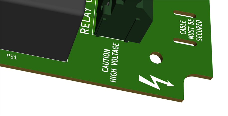
For instance, here's a different project, where I put the project PCB into an enclosure (non-extruded in this case). This project doesn't have a front panel, but I could easily make one if needed, using the method described.

image

Thanks for reading!

  • Sign in to reply
  • Cancel

Top Replies

  • Andrew J
    Andrew J over 2 years ago +4
    I created 4 different panels in this way following your earlier effort. It’s such a good idea and the finished results look great. Range of colours with JLCPCB too. I have two tips if using JLCPCB; …
  • shabaz
    shabaz over 2 years ago in reply to Andrew J +3
    Found it here .. I'm going to remember is as 4 JLC's ... also need to click on " Specify a Location ". I wish they would optionally accept a file (e.g. JSON, YAML or whatever) with all their config settings…
  • baldengineer
    baldengineer over 2 years ago +2
    I usually import SVG instead of DXF in KiCad. In the past, I had trouble with it not handling curves very well. SVG hasn't been perfect either, however. I sometimes have to apply a scaling factor. So…
  • shabaz
    shabaz over 2 years ago

    (This should really be a blog, but I accidentally made it a forum entry. Is it possible to change it cstanton or is it fixed as a forum entry? (I looked at Move, but I think that doesn't change to a blog). If it's not possible that's fine, but if it is possible, that would be good!

    • Cancel
    • Vote Up 0 Vote Down
    • Sign in to reply
    • Cancel
  • dougw
    dougw over 2 years ago

    Presumably the entire drawing could be done as a DXF, including text.

    It brings up the age old question - should the mechanical design accommodate the electrical design or should the electrical design fit the mechanical design?

    • Cancel
    • Vote Up +1 Vote Down
    • Sign in to reply
    • Cancel
  • baldengineer
    baldengineer over 2 years ago

    I usually import SVG instead of DXF in KiCad. In the past, I had trouble with it not handling curves very well.

    SVG hasn't been perfect either, however. I sometimes have to apply a scaling factor. So I always add a 10 mm line so I can scale correctly.

    Also, here is a tip I recently learned and REALLY liked. Don't import your graphic directly into the PCB. Instead, create it as a footprint. That way, if you need to update the artwork, it is much easier to replace it in the footprint and update the footprint on the PCB.

    • Cancel
    • Vote Up +2 Vote Down
    • Sign in to reply
    • Cancel
  • shabaz
    shabaz over 2 years ago in reply to dougw

    Hi Doug,

    I believe it could, and would be a better way for those familiar with (say) Inkscape or any CAD package.

    In my case, I don't have any 2D CAD package that I know how to use (and I can barely do anything with FreeCAD or Inkscape) so preferred to do as much in the KiCad editor, i.e. just use the enclosure manufacturer's DXF file imported in as a drawing layer and overlay with my own cut lines and silkscreen where needed.

    I liked old AutoSketch and old AutoCAD, and the excellent Generic CADD (it was a DOS application) but I've forgotten how to use them (and don't have copies of them any longer).

    • Cancel
    • Vote Up 0 Vote Down
    • Sign in to reply
    • Cancel
  • shabaz
    shabaz over 2 years ago in reply to baldengineer

    Hi James,

    I saw some DXF decode failure artifacts too, I wonder what causes them. For the front panel use-case it wasn't an issue since I was only concerned with the outline, but it would be nice if that was resolved. Inkscape managed to read the DXF file perfectly, so it wasn't a faulty DXF file. The main benefit of the DXF was that the measurements were accurate, since it was the manufacturer's file, so no scaling needed. I much prefer SVG for vector too!

    image

    It's awesome how easy graphics are with KiCad. It was a lot harder with EAGLE. I've been using the graphics import for high-voltage symbols today; they might already exist but it was quick to do it anyway:

    image

    • Cancel
    • Vote Up +1 Vote Down
    • Sign in to reply
    • Cancel
  • baldengineer
    baldengineer over 2 years ago in reply to shabaz

    Agreed. V6 made some significant improvements with graphics handling. And from what I've read, V7 takes a few more steps forward as well.

    • Cancel
    • Vote Up +1 Vote Down
    • Sign in to reply
    • Cancel
  • Jan Cumps
    Jan Cumps over 2 years ago in reply to shabaz

    If moving is not possible, you can copy the source code (Edit -> Tools -> Source code), copy

    Then create a blog, follow the same steps, paste

    • Cancel
    • Vote Up +1 Vote Down
    • Sign in to reply
    • Cancel
  • Andrew J
    Andrew J over 2 years ago

    I created 4 different panels in this way following your earlier effort.  It’s such a good idea and the finished results look great.  Range of colours with JLCPCB too.  I have two tips if using JLCPCB;

    1. On the hidden side of the panel, put the text ‘JLCPCBJLCPCBJLCPCB” without the quotes.  This is where they will print a serial number and you don’t really want it on the front side.  I can’t remember the exact number of iterations of JLCPCB but it says on their gerber import web page.  Also make sure to tick the right option on that page.
    2. If there is no copper on the hidden side - highly likely as you are just creating cut outs, but there may be a grounding point for example - Kicad will generate an empty gerber file for that and JLCPCB gerber import will flag up a problem.  It’s perfectly valid to have an empty file but there must be a bug on their website.  You will need to drop them a note to tell them this is correct, or wait for someone to contact you for clarification.
    • Cancel
    • Vote Up +4 Vote Down
    • Sign in to reply
    • Cancel
  • cstanton
    cstanton over 2 years ago in reply to shabaz
    shabaz said:
    Is it possible to change it

    Unfortunately not.

    shabaz said:
    is it fixed as a forum entry?

    Unfortunately so.

    • Cancel
    • Vote Up +1 Vote Down
    • Sign in to reply
    • Cancel
  • shabaz
    shabaz over 2 years ago in reply to Andrew J

    Hi Andrew,

    Thanks for these tips! I had been wondering how to get the serial number moved. Interestingly on a recent order, JLCPCB placed the serial number on the bottom layer without being prompted, and it was intended to be a front panel, so I guess one of the manual inspectors was attentive there! I'll be adding that text from now on though, to eliminate the risk.

    • Cancel
    • Vote Up 0 Vote Down
    • Sign in to reply
    • Cancel
>
element14 Community

element14 is the first online community specifically for engineers. Connect with your peers and get expert answers to your questions.

  • Members
  • Learn
  • Technologies
  • Challenges & Projects
  • Products
  • Store
  • About Us
  • Feedback & Support
  • FAQs
  • Terms of Use
  • Privacy Policy
  • Legal and Copyright Notices
  • Sitemap
  • Cookies

An Avnet Company © 2025 Premier Farnell Limited. All Rights Reserved.

Premier Farnell Ltd, registered in England and Wales (no 00876412), registered office: Farnell House, Forge Lane, Leeds LS12 2NE.

ICP 备案号 10220084.

Follow element14

  • X
  • Facebook
  • linkedin
  • YouTube