element14 Community
element14 Community
    Register Log In
  • Site
  • Search
  • Log In Register
  • About Us
  • Community Hub
    Community Hub
    • What's New on element14
    • Feedback and Support
    • Benefits of Membership
    • Personal Blogs
    • Members Area
    • Achievement Levels
  • Learn
    Learn
    • Ask an Expert
    • eBooks
    • element14 presents
    • Learning Center
    • Tech Spotlight
    • STEM Academy
    • Webinars, Training and Events
    • Learning Groups
  • Technologies
    Technologies
    • 3D Printing
    • FPGA
    • Industrial Automation
    • Internet of Things
    • Power & Energy
    • Sensors
    • Technology Groups
  • Challenges & Projects
    Challenges & Projects
    • Design Challenges
    • element14 presents Projects
    • Project14
    • Arduino Projects
    • Raspberry Pi Projects
    • Project Groups
  • Products
    Products
    • Arduino
    • Avnet Boards Community
    • Dev Tools
    • Manufacturers
    • Multicomp Pro
    • Product Groups
    • Raspberry Pi
    • RoadTests & Reviews
  • Store
    Store
    • Visit Your Store
    • Choose another store...
      • Europe
      •  Austria (German)
      •  Belgium (Dutch, French)
      •  Bulgaria (Bulgarian)
      •  Czech Republic (Czech)
      •  Denmark (Danish)
      •  Estonia (Estonian)
      •  Finland (Finnish)
      •  France (French)
      •  Germany (German)
      •  Hungary (Hungarian)
      •  Ireland
      •  Israel
      •  Italy (Italian)
      •  Latvia (Latvian)
      •  
      •  Lithuania (Lithuanian)
      •  Netherlands (Dutch)
      •  Norway (Norwegian)
      •  Poland (Polish)
      •  Portugal (Portuguese)
      •  Romania (Romanian)
      •  Russia (Russian)
      •  Slovakia (Slovak)
      •  Slovenia (Slovenian)
      •  Spain (Spanish)
      •  Sweden (Swedish)
      •  Switzerland(German, French)
      •  Turkey (Turkish)
      •  United Kingdom
      • Asia Pacific
      •  Australia
      •  China
      •  Hong Kong
      •  India
      •  Korea (Korean)
      •  Malaysia
      •  New Zealand
      •  Philippines
      •  Singapore
      •  Taiwan
      •  Thailand (Thai)
      • Americas
      •  Brazil (Portuguese)
      •  Canada
      •  Mexico (Spanish)
      •  United States
      Can't find the country/region you're looking for? Visit our export site or find a local distributor.
  • Translate
  • Profile
  • Settings
PCB Design, Prototyping and Production
  • Products
  • More
PCB Design, Prototyping and Production
PCB Forum PCB use of "vias" on high speed signal path
  • Blog
  • Forum
  • Documents
  • Leaderboard
  • Files
  • Members
  • Mentions
  • Sub-Groups
  • Tags
  • More
  • Cancel
  • New
Join PCB Design, Prototyping and Production to participate - click to join for free!
Actions
  • Share
  • More
  • Cancel
Forum Thread Details
  • Replies 4 replies
  • Subscribers 120 subscribers
  • Views 1718 views
  • Users 0 members are here
  • high speed
  • via
  • pcb design
Related

PCB use of "vias" on high speed signal path

gyuunyuu1989
gyuunyuu1989 over 2 years ago

High speed signals require impedance matching. Basically this means that the signal path must have a continuos impedance throughout which is matched with the receiver impedance. This is to prevent signal reflections that can corrupt the signal. In very basic language, the PCB track characteristic impedance depends on the track width, track copper height, distance from the reference GND plane and dielectric constant. Depending on the layer stackup, the user can calculate a track width to get target impedance in the CAD tool. This topic is clear to me.

Now lets come to vias. There are several issues with vias. Via is a 90 deg turn in signal path. Via geometry means that the signal path is different from a PCB track. Via does not have a reference plane by default. The geometry and lack of reference plane means that the via impedance will usually be not matched with the PCB track. This can lead to signal reflection and thus compromise the signal integrity.

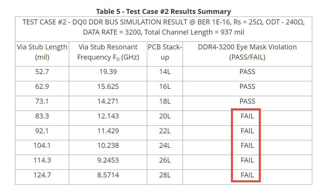
Assume that we are doing PCB design for these: DDR3, DD4, PCIe gen 4 and the tracks.

So people that say via affect is small since its size is would be than wavelength. Some people say that we should put some stitiching vias nearby (don't know how far) and leave it at that and it should not cause massive problem.

It is not possible to completely avoid using vias. The basic question thus is as follows: when it is needed to use via, do we use any (small) size via and just hope that it works? Or do we need to design via with specific geometry and put a specific number of GND stitching vias close to it to give a return path for the current? Designing vias requires use of advanced tools which are called 3D solvers.

The question just aims to understand the correct approach to using via in high speed boards. Please note that I am an electronic engineer by profession, I have designed simpler PCBs in the past (2 - 4 layers) but not high speed stuff like DDR3 and transceivers. I am trying to gather the theoretical knowledge for high speed designs.

  • Sign in to reply
  • Cancel

Top Replies

  • shabaz
    shabaz over 2 years ago in reply to misaz +4
    I think you misunderstood my comment; it agrees with yours. The question from the poster was " do we use any (small) size via and just hope that it works? ", and the answer to that is no, at least not…
  • charlieo21
    charlieo21 over 2 years ago +2
    Never hope that your design is going to work the first time. I don't have experience with high-speed signals like DDR3, but I know there is a great book about that topic: High Speed Signal Propagation…
  • misaz
    misaz over 2 years ago in reply to shabaz +1
    I originaly thought the same but last year I attended webinar describing vias on very high speed deesigns ( https://www.doulos.com/webinars/signal-integrity-pcb-vias-and-remedies/ ). Experienced speaker…
Parents
  • shabaz
    shabaz over 2 years ago

    Hi,

    Here's a comment unless you get a better answer:

    No, with DDR4 you can't just assume it will work by just inserting any via. I'm not a PCB designer, it's not my chosen career. But even I'm pretty sure you need to research a whole load if you're serious about working with this technology, way more than a comment could hope to achieve. You probably should be reading articles such as this one, and following up each reference there: https://www.signalintegrityjournal.com/articles/1731-signal-integrity-characterization-of-via-stubs-on-high-speed-ddr4-channels

    There are plenty of other articles on that site that I think you should definitely be studying if this is your career.

    • Cancel
    • Vote Up 0 Vote Down
    • Sign in to reply
    • Cancel
  • misaz
    misaz over 2 years ago in reply to shabaz

    I originaly thought the same but last year I attended webinar describing vias on very high speed deesigns (https://www.doulos.com/webinars/signal-integrity-pcb-vias-and-remedies/). Experienced speaker presented that vias are possible on the high speed signal and introduced signal integrity issues can be modeled as well as measured. Quality depdends on via length (how many layers via travel). For example shorter via between internal layers behave better than via between outer layers, and special types of vias (blind, backdrilled) are almost always needed.

    • Cancel
    • Vote Up +1 Vote Down
    • Sign in to reply
    • Cancel
Reply
  • misaz
    misaz over 2 years ago in reply to shabaz

    I originaly thought the same but last year I attended webinar describing vias on very high speed deesigns (https://www.doulos.com/webinars/signal-integrity-pcb-vias-and-remedies/). Experienced speaker presented that vias are possible on the high speed signal and introduced signal integrity issues can be modeled as well as measured. Quality depdends on via length (how many layers via travel). For example shorter via between internal layers behave better than via between outer layers, and special types of vias (blind, backdrilled) are almost always needed.

    • Cancel
    • Vote Up +1 Vote Down
    • Sign in to reply
    • Cancel
Children
  • shabaz
    shabaz over 2 years ago in reply to misaz

    I think you misunderstood my comment; it agrees with yours.

    The question from the poster was "do we use any (small) size via and just hope that it works?", and the answer to that is no, at least not for DDR4.

    The suggestion isn't that vias are not possible, it's just that one cannot arbitrarily insert a via and hope it will work. The web link mentions this and shows what happens, which is what I think you're also mentioning:

    image

    • Cancel
    • Vote Up +4 Vote Down
    • Sign in to reply
    • Cancel
element14 Community

element14 is the first online community specifically for engineers. Connect with your peers and get expert answers to your questions.

  • Members
  • Learn
  • Technologies
  • Challenges & Projects
  • Products
  • Store
  • About Us
  • Feedback & Support
  • FAQs
  • Terms of Use
  • Privacy Policy
  • Legal and Copyright Notices
  • Sitemap
  • Cookies

An Avnet Company © 2025 Premier Farnell Limited. All Rights Reserved.

Premier Farnell Ltd, registered in England and Wales (no 00876412), registered office: Farnell House, Forge Lane, Leeds LS12 2NE.

ICP 备案号 10220084.

Follow element14

  • X
  • Facebook
  • linkedin
  • YouTube