


Hi everyone,
I am struggling with a Monolithic Power MP2172 'buck' switching IC design.
The manufacturer's data sheet (page 15) shows a 'recommended' pcb layout but it is confusing as the picture has 'vias' that appear to be going nowhere?
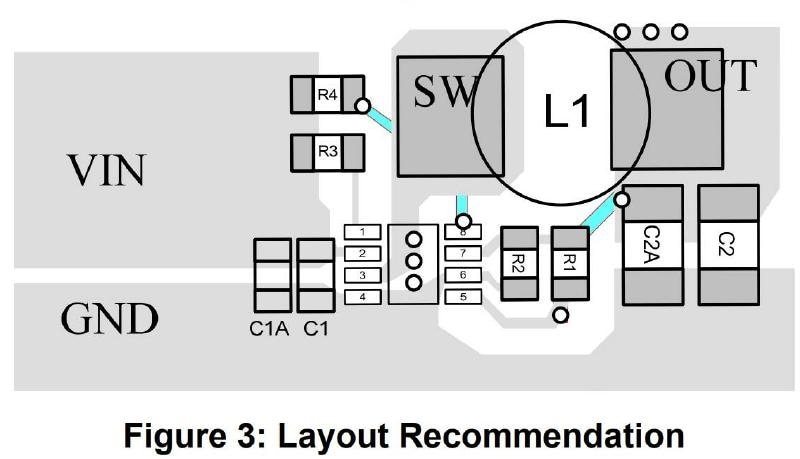
It looks as though the layout is a double sided board as there are a couple of (coloured blue) tracks that must be on the bottom.
However there are 'vias' under the IC that appear to go nowhere unless there is a ground plane or other layer?
There are also 3 'vias' at the top of the OUT copper that don't make sense either, if there is no plane beneath.
So:-
I generated my own layout which was being added to a double sided board with a top and bottom side ground plane.
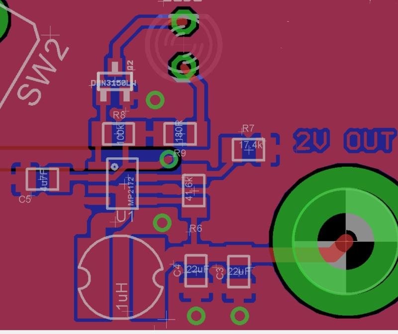
The 'switcher is to generate 2V dc from a single LiPo battery, I calculated the correct values for the FB divider and had my board made.
Sadly when populated the switching converter only produced 0.5V.
A quick 'scope around the IC found a 4 step staircase waveform on the SW pin, as though the IC was trying to start and failing.
Further investigation revealed my supply input decoupling was only 4.7uF instead of the recommended 2 x 10uF...doooh!
I replaced the capacitor with a 22uF and a 100nF in parallel which improved the situation by now producing 1.3V and a much larger 25 step staircase switching waveform.
However still not getting up to full operation.
I then tried drilling extra via holes next to the grounded end of the input decoupling capacitors and 'pinned' this point with a through wire to the GND plane on the bottom
layer, Thinking I had a high impedance GND or ground loop.
This stopped the switching completely!
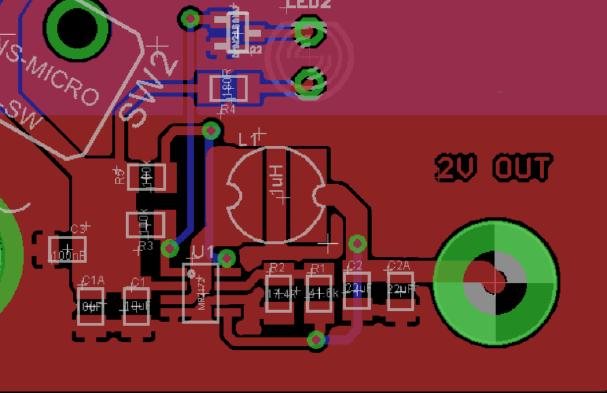
I have since reworked my layout (below) making it as close to the recommended one, and, pared back the bottom layer ground plane from beneath the switcher.
But before I get a new board made I could do with advice from someone who has experience with this family of switching IC's and in particular the MP2172.
Please help if you can..:-)
Thanks in anticipation
Dave

