element14 Community
element14 Community
    Register Log In
  • Site
  • Search
  • Log In Register
  • About Us
  • Community Hub
    Community Hub
    • What's New on element14
    • Feedback and Support
    • Benefits of Membership
    • Personal Blogs
    • Members Area
    • Achievement Levels
  • Learn
    Learn
    • Ask an Expert
    • eBooks
    • element14 presents
    • Learning Center
    • Tech Spotlight
    • STEM Academy
    • Webinars, Training and Events
    • Learning Groups
  • Technologies
    Technologies
    • 3D Printing
    • FPGA
    • Industrial Automation
    • Internet of Things
    • Power & Energy
    • Sensors
    • Technology Groups
  • Challenges & Projects
    Challenges & Projects
    • Design Challenges
    • element14 presents Projects
    • Project14
    • Arduino Projects
    • Raspberry Pi Projects
    • Project Groups
  • Products
    Products
    • Arduino
    • Avnet Boards Community
    • Dev Tools
    • Manufacturers
    • Multicomp Pro
    • Product Groups
    • Raspberry Pi
    • RoadTests & Reviews
  • Store
    Store
    • Visit Your Store
    • Choose another store...
      • Europe
      •  Austria (German)
      •  Belgium (Dutch, French)
      •  Bulgaria (Bulgarian)
      •  Czech Republic (Czech)
      •  Denmark (Danish)
      •  Estonia (Estonian)
      •  Finland (Finnish)
      •  France (French)
      •  Germany (German)
      •  Hungary (Hungarian)
      •  Ireland
      •  Israel
      •  Italy (Italian)
      •  Latvia (Latvian)
      •  
      •  Lithuania (Lithuanian)
      •  Netherlands (Dutch)
      •  Norway (Norwegian)
      •  Poland (Polish)
      •  Portugal (Portuguese)
      •  Romania (Romanian)
      •  Russia (Russian)
      •  Slovakia (Slovak)
      •  Slovenia (Slovenian)
      •  Spain (Spanish)
      •  Sweden (Swedish)
      •  Switzerland(German, French)
      •  Turkey (Turkish)
      •  United Kingdom
      • Asia Pacific
      •  Australia
      •  China
      •  Hong Kong
      •  India
      •  Korea (Korean)
      •  Malaysia
      •  New Zealand
      •  Philippines
      •  Singapore
      •  Taiwan
      •  Thailand (Thai)
      • Americas
      •  Brazil (Portuguese)
      •  Canada
      •  Mexico (Spanish)
      •  United States
      Can't find the country/region you're looking for? Visit our export site or find a local distributor.
  • Translate
  • Profile
  • Settings
RoadTests & Reviews
  • Products
  • More
RoadTests & Reviews
Blog Blog 1: Road test Digilent ARTY Z7 Dev Board
  • Blog
  • RoadTest Forum
  • Documents
  • RoadTests
  • Reviews
  • Polls
  • Files
  • Members
  • Mentions
  • Sub-Groups
  • Tags
  • More
  • Cancel
  • New
Join RoadTests & Reviews to participate - click to join for free!
  • Share
  • More
  • Cancel
  • Author Author: anupash.1002
  • Date Created: 6 Oct 2018 3:00 PM Date Created
  • Views 1694 views
  • Likes 4 likes
  • Comments 5 comments
Related
Recommended
  • digilent arty z7 dev board
  • roadtest; roadtest
  • fpga

Blog 1: Road test Digilent ARTY Z7 Dev Board

anupash.1002
anupash.1002
6 Oct 2018

Here I tried to learn different methods to program the Digilent ARTY Z7 Dev Board. One simple way is to program .vhdl file in the Vivado and then create the sdk. Another way is to create the Block diagram in the vivado and then export the hardware to the SK.


  • VHDL code program on ARTY Z7
  • Vivado Block Diagram design to program ARTY Z7 FPGA
  • LED, button and SW in VivadoSDK to program ARTY Z7 FPGA


VHDL code program on ARTY Z7


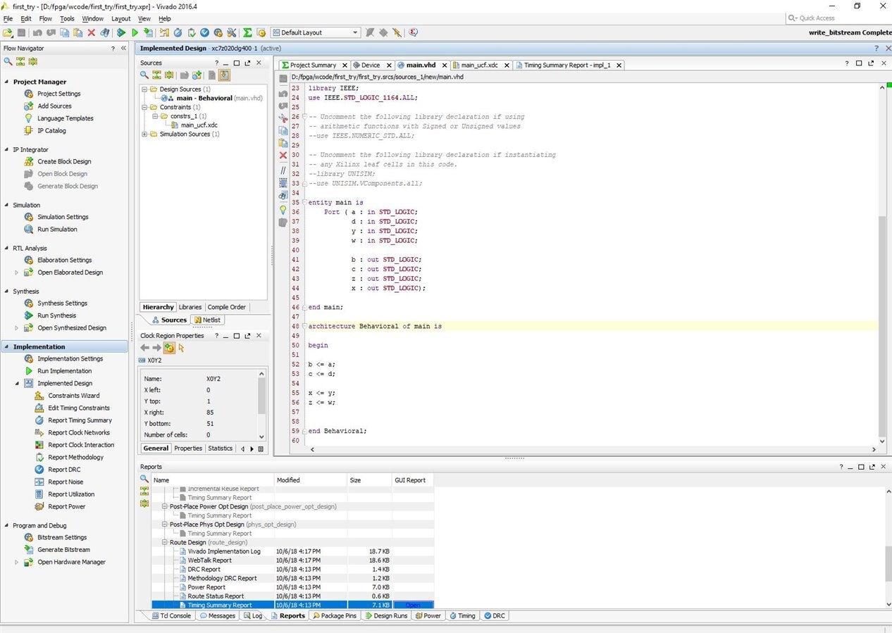
Here I have a simple .vhdl code and I programmed the fpga.The aim is to light 4 leds by pushing the 4 buttons on the dev board. I also took the necessary part from GITHUB and wrote the constraints file .xdc


image


image

Writing appropriate .xdc file to manage the constraints


set_property -dict { PACKAGE_PIN R14 IOSTANDARD LVCMOS33 } [get_ports { b }]; #Sch=LED0

set_property -dict { PACKAGE_PIN P14
IOSTANDARD LVCMOS33 } [get_ports { c }]; #Sch=LED1

set_property -dict { PACKAGE_PIN N16
IOSTANDARD LVCMOS33 } [get_ports { x }]; #Sch=LED2

set_property -dict { PACKAGE_PIN M14
IOSTANDARD LVCMOS33 } [get_ports { z }]; #Sch=LED3


set_property -dict { PACKAGE_PIN D19
IOSTANDARD LVCMOS33 } [get_ports { a }]; #Sch=BTN0

set_property -dict { PACKAGE_PIN D20
IOSTANDARD LVCMOS33 } [get_ports { d }]; #Sch=BTN1

set_property -dict { PACKAGE_PIN L20
IOSTANDARD LVCMOS33 } [get_ports { y }]; #Sch=BTN2

set_property -dict { PACKAGE_PIN L19
IOSTANDARD LVCMOS33 } [get_ports { w }]; #Sch=BTN3


image

This error appeared many times after reset and sometimes during on. Then you must re-fresh the project and if not then re-power the board again. At some point I thought the board is broken. But it is not true the FPGA became very hot and after I left turned off for few hours it was running good again.


Another mistake I also made often is the programming jumper should be set correctly to JTAG-QSPI to program bitstream.


After re-starting the Vivado 2016


image

Looking at Implementation of the code on FPGA


image

image

Details in the timing report. Luckily no timing failures for this simple project. Else it must be checked here


image

Going deeper and looking into the Schematics created from the VHDL code


image

Programming the bit-stream file on fpga dev board.


You don't have permission to edit metadata of this video.
Edit media
x
image
Upload Preview
image


Here the vivado SDK was not used to run the code on FPGA.


Vivado Block Diagram design to program ARTY Z7 FPGA


In this mini-project I did not write an fpga code but connected the leds and push buttons using the Block Diagram from Vivado and added as GPIOs. The control of the LEDs and push buttons in done in SDK software. The results I also sent in serial port TeraTERM to see which button was pushed for which led is ON. When using this approach the .xdc file (constraints file for the hardware on the fpga) may not be manually written.


image


image


You don't have permission to edit metadata of this video.
Edit media
x
image
Upload Preview
image

Testing with the Vivado SDK 2016


LED, button and SW in VivadoSDK to program ARTY Z7 FPGA


Further the block diagram creation approach is used to control the push buttons, leds and the two switches on the FPGA board. The outputs of the on board switches are sent to Tera Term serial port to see the current status.


image

The Block Diagram implementation


image


After generating the bitstream, I exported the hardware to the Vivado SDK. And the control of the leds and push button is written in the SDK software using C language.


image

image

Finally programming the FPGA ARTY Z7 board from the Vivado SDK.


You don't have permission to edit metadata of this video.
Edit media
x
image
Upload Preview
image


As seen I also had the issue when programming the VivadoSDK code on the Digilent Arty-Z7.


The AP transaction error, DAP status f0000021 error and Memory write error at 0x100000. AP transaction timeout are also common when programming the fpga.


The only work out on the Digilent forum as written is


  • The boot mode jumper must be set to JTAG
  • Press the PORB button for sometime, and only then Program FPGA.
  • Re-Launch or re-program from VivadoSDK menu on the FPGA Hardware to work.
  • Sign in to reply

Top Comments

  • DAB
    DAB over 6 years ago in reply to anupash.1002 +3
    I started as an Electronics Technician and then took a BS in Computer Engineering which was a split Hardware/software degree. The knowledge I gained served me well as I could always understand both sides…
  • DAB
    DAB over 6 years ago +1
    Nice post. The whole issue with FPGA is that you implement very specific hardware circuits. If all you know is software, you need to shift into a different mind set and begin to understand the details…
  • DAB
    DAB over 6 years ago in reply to anupash.1002 +1
    By the time I was thirty I was designing bit slice circuits and building advanced microprocessor signal processing algorithms. Dive in the water's fine. DAB
  • DAB
    DAB over 6 years ago in reply to anupash.1002

    By the time I was thirty I was designing bit slice circuits and building advanced microprocessor signal processing algorithms.


    Dive in the water's fine.


    DAB

    • Cancel
    • Vote Up +1 Vote Down
    • Sign in to reply
    • More
    • Cancel
  • anupash.1002
    anupash.1002 over 6 years ago

    Thanks DAB for your insight info on fpga approach.

    Looks like a long way for me to go. Well I am only 30 so that can work

    • Cancel
    • Vote Up 0 Vote Down
    • Sign in to reply
    • More
    • Cancel
  • DAB
    DAB over 6 years ago in reply to anupash.1002

    I started as an Electronics Technician and then took a BS in Computer Engineering which was a split Hardware/software degree.

    The knowledge I gained served me well as I could always understand both sides of any system.


    The FPGA evolution enabled engineers to implement complex hardware logic in a single device as opposed to lots of integrated circuits.

    The GPGA approach was faster and more easily updated verses the traditional circuit board approach.

    Latter they became essential for replacing obsolete circuits and IC's to keep legacy systems working.


    Once you master the FPGA approach, it enables you to build intricate logic circuits in a small package, especially where size and timing issues dominate.

    There are a lot of communication protocols that require fast data decoding and encoding and you just cannot meet the timing with a software approach.

    The FPGA enables you to translate your software protocol into a logic circuit and then change the design as the protocol evolves.


    DAB

    • Cancel
    • Vote Up +3 Vote Down
    • Sign in to reply
    • More
    • Cancel
  • anupash.1002
    anupash.1002 over 6 years ago in reply to DAB

    Thank you DAB. yes my issue was that there was so much happening in hardware although everything is well documented if one synthesis fails or a part of the design failed due to .xdc I was not able to catch the problem so easily.


    I had never thought that for issues re-starting is the only solution.


    It seems you need good knowledge of hardware and software to get everything done or 2 separate engineers.

    • Cancel
    • Vote Up 0 Vote Down
    • Sign in to reply
    • More
    • Cancel
  • DAB
    DAB over 6 years ago

    Nice post.

    The whole issue with FPGA is that you implement very specific hardware circuits.

    If all you know is software, you need to shift into a different mind set and begin to understand the details of hardware design.


    It is very different from software design, but the logic steps are similar enough for you to understand what happens.

    You just need to learn how hardware design works and then you have to learn what the tools provide enable you to do.

    All of that will take you some time and effort.


    DAB

    • Cancel
    • Vote Up +1 Vote Down
    • Sign in to reply
    • More
    • Cancel
element14 Community

element14 is the first online community specifically for engineers. Connect with your peers and get expert answers to your questions.

  • Members
  • Learn
  • Technologies
  • Challenges & Projects
  • Products
  • Store
  • About Us
  • Feedback & Support
  • FAQs
  • Terms of Use
  • Privacy Policy
  • Legal and Copyright Notices
  • Sitemap
  • Cookies

An Avnet Company © 2025 Premier Farnell Limited. All Rights Reserved.

Premier Farnell Ltd, registered in England and Wales (no 00876412), registered office: Farnell House, Forge Lane, Leeds LS12 2NE.

ICP 备案号 10220084.

Follow element14

  • X
  • Facebook
  • linkedin
  • YouTube