element14 Community
element14 Community
    Register Log In
  • Site
  • Search
  • Log In Register
  • Members
    Members
    • Benefits of Membership
    • Achievement Levels
    • Members Area
    • Personal Blogs
    • Feedback and Support
    • What's New on element14
  • Learn
    Learn
    • Learning Center
    • eBooks
    • STEM Academy
    • Webinars, Training and Events
    • Learning Groups
  • Technologies
    Technologies
    • 3D Printing
    • FPGA
    • Industrial Automation
    • Internet of Things
    • Power & Energy
    • Sensors
    • Technology Groups
  • Challenges & Projects
    Challenges & Projects
    • Design Challenges
    • element14 presents
    • Project14
    • Arduino Projects
    • Raspberry Pi Projects
    • Project Groups
  • Products
    Products
    • Arduino
    • Dev Tools
    • Manufacturers
    • Raspberry Pi
    • RoadTests & Reviews
    • Avnet Boards Community
    • Product Groups
  • Store
    Store
    • Visit Your Store
    • Choose Another Store
      • Europe
      •  Austria (German)
      •  Belgium (Dutch, French)
      •  Bulgaria (Bulgarian)
      •  Czech Republic (Czech)
      •  Denmark (Danish)
      •  Estonia (Estonian)
      •  Finland (Finnish)
      •  France (French)
      •  Germany (German)
      •  Hungary (Hungarian)
      •  Ireland
      •  Israel
      •  Italy (Italian)
      •  Latvia (Latvian)
      •  
      •  Lithuania (Lithuanian)
      •  Netherlands (Dutch)
      •  Norway (Norwegian)
      •  Poland (Polish)
      •  Portugal (Portuguese)
      •  Romania (Romanian)
      •  Russia (Russian)
      •  Slovakia (Slovak)
      •  Slovenia (Slovenian)
      •  Spain (Spanish)
      •  Sweden (Swedish)
      •  Switzerland(German, French)
      •  Turkey (Turkish)
      •  United Kingdom
      • Asia Pacific
      •  Australia
      •  China
      •  Hong Kong
      •  India
      •  Korea (Korean)
      •  Malaysia
      •  New Zealand
      •  Philippines
      •  Singapore
      •  Taiwan
      •  Thailand (Thai)
      • Americas
      •  Brazil (Portuguese)
      •  Canada
      •  Mexico (Spanish)
      •  United States
      Can't find the country/region you're looking for? Visit our export site or find a local distributor.
  • Translate
  • Profile
RoadTests & Reviews
  • Products
  • More
RoadTests & Reviews
Blog PI BridgeSwitch roadtest preview – Design a good PCB heat flow using FEM approach
  • Blog
  • RoadTest Forum
  • Documents
  • Events
  • RoadTests
  • Reviews
  • Mentions
  • Sub-Groups
  • Tags
  • More
  • Cancel
  • New
  • femm
  • BridgeSwitch
  • Subscribe by email
  • More
  • Cancel
  • Share
  • Subscribe by email
  • More
  • Cancel
Related
Recommended

PI BridgeSwitch roadtest preview – Design a good PCB heat flow using FEM approach

federicoma
federicoma
14 Dec 2021

Starting a new pcb design, featuring the PI BridgeSwitch, require a deep thermal management analysis, expecially if you want to avoid the heatsink in your design. A nice step forward should be to simulate the PCB heat flow and design a PCB with the correct dimension of the copper area to dissipate the BridgeSwitch heating.

One solution could be to use FEMM, a free software:
https://www.femm.info

Another way could be to use Ansys suite, the nice thing here is there’s a free student opportunity to download the software:
https://www.ansys.com/it-it/academic/students/ansys-electronics-desktop-student

I tried the free software solution, using FEMM, but I didn’t understand how to complete the workflow.
This was my steps, does anyone can make a step forward? If you want to try, these is my work, so far:

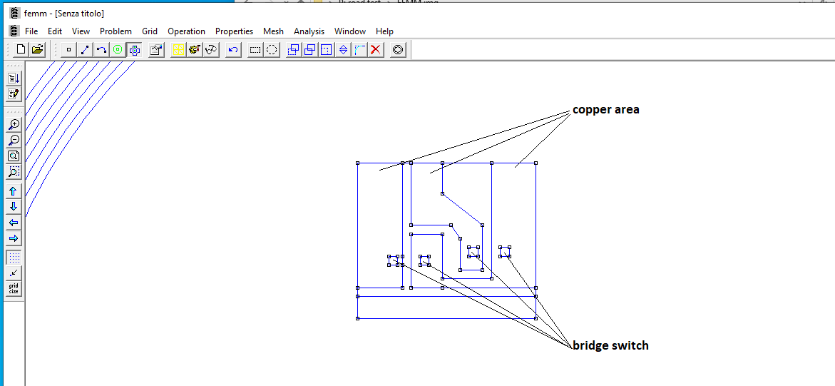
note: The FEMM software can work just with one PCB side, not both top and bottom, so I think the getting start point could be the RDR-873 board, which is mainly at bottom side. I did some reverse engineering and get the PCB layout to a DXF.

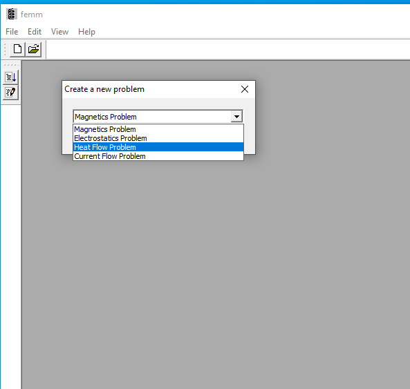
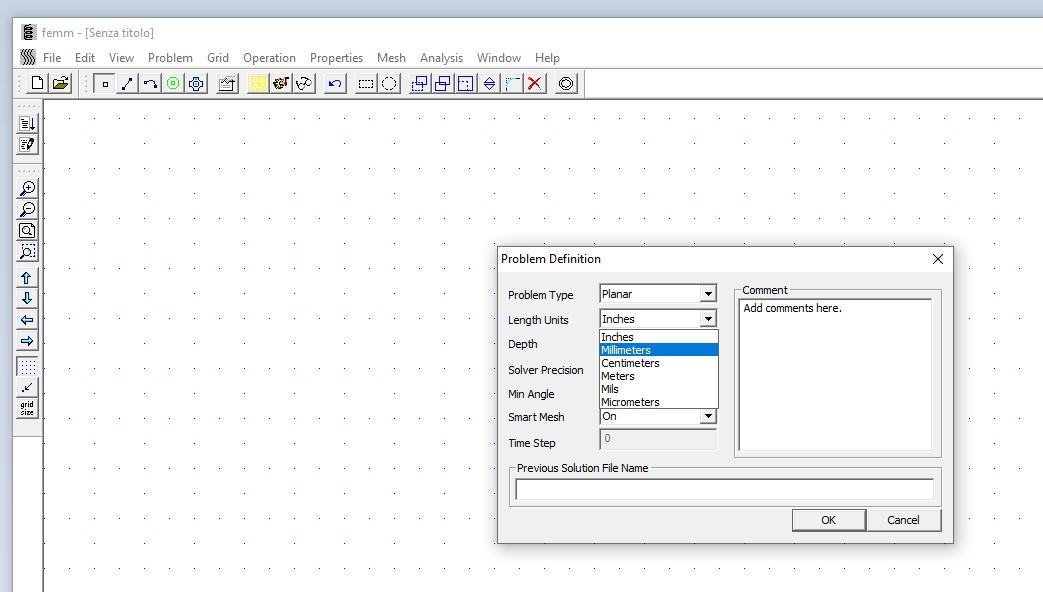
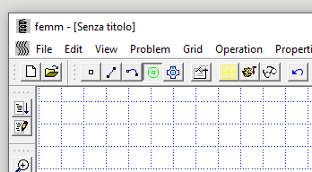
1) Open FEMM, create a new heat flow problem and set the problem to millimeters, clicking on problem ..

femm_01 image

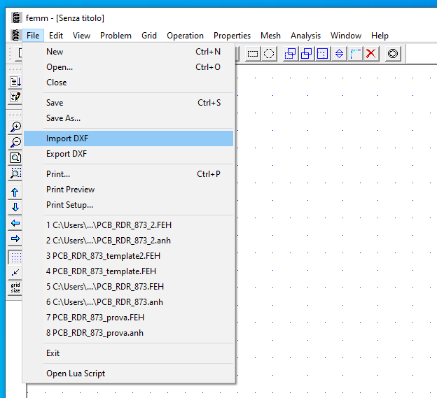
2) Import the dxf from the attached file “rdr-873.dxf” 
hints: don’t change the tolerance and then press the zoom out since you see the board moving the zoom area with the keyboard arrows.

img03

3) Now you get the same situation of these images, with some simplification. Please consider the left on top view, so the bottom is mirrored.

image image

Let’s understand what we get

image

4) Import some well known materials properties:
Properties – Materials library – Metallic solid – Copper pure (drag to the right)
Properties – Materials library – Gases at 1atm – Air (drag to the right)
Properties – Materials library – Non metallic – Plaster (drag to the right)

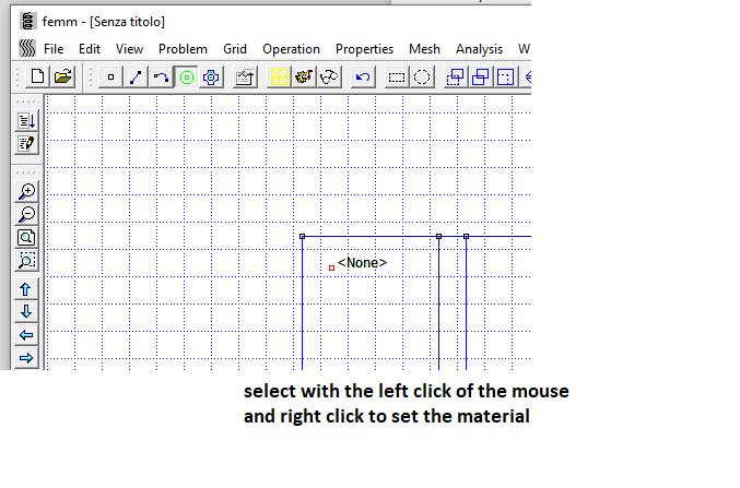
5) Set the region material using the green button

image

6) setup the material

image

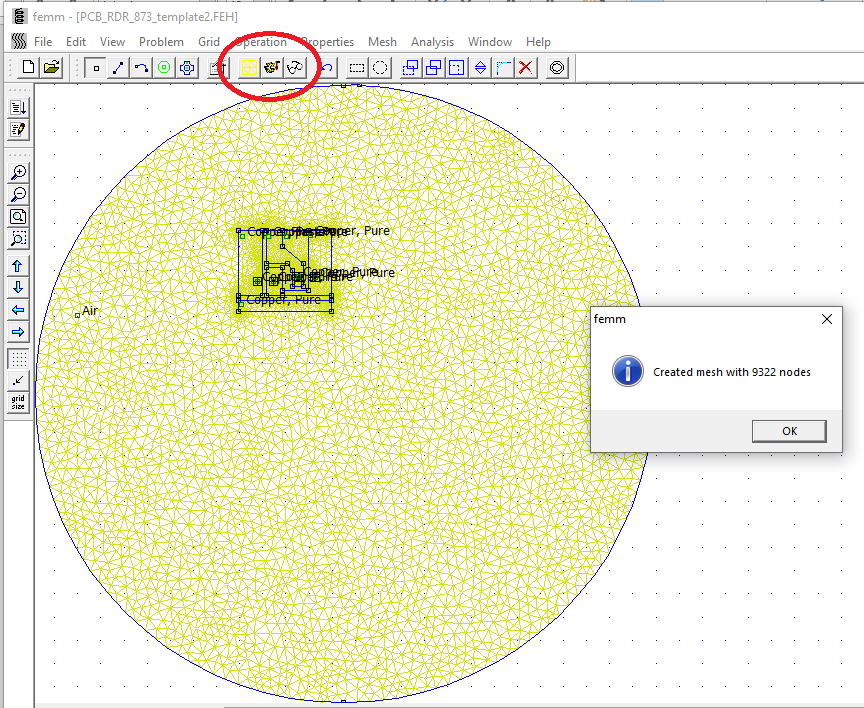
7) Now you should have the same situation of the attached file “PCB_RDR_873_template2.FEH”
This situation is a starting point. If you try to solve the problem, there will be not an end because the missing of the right boundary conditions.
Let’s open another attached file, PCB_RDR_873_2.FEH, this have a boundary condition that ends to a solved problem, but the result is not usefull.
If you want to see,
press the mesh button, and then the right one close button to solve the problem, and finally the lens to see the result.
It seems the whole board is at the same temperature, it can't be true.

image image

I’m stuck there: the problem can’t be solved because the boundary conditions are not correctly setup.
I’m getting inside this to understand how to setup the situation, if anybody wold like to discuss with me how to proceed, it should be very helpful.
I’m studying this tutorial now:

https://www.femm.info/wiki/HeatFlowTutorial

attached_files.zip
  • Sign in to reply
  • federicoma
    federicoma over 1 year ago in reply to jc2048

    Hi jc2048, thank so much for your very interesting reply.
    That's nice to be in touch with this great people, thanks to e14 community for that.

    The FEMM software is a very good resource, I use it daily, but for magnetics purpose.
    I use FEMM calling the operation using OctaveFEMM, it's a MATLAB language like scripting. Very nice and free.
    That's why I don't use the UI so much, don't even know it too much.
    A lot of people use LUA script or Python, maybe that's the best choice, I chose OctaveFEMM because I'm a daily MATLAB user.

    For the simulation, that's true, I was wrong putting 60°C, so I fixed that, thankyou.
    Nice idea for the boundary condition at the edge of the board.
    You're so right thinking about the heat dissipation mechanism, maybe this work will be not usefull. I think that's the end of this trial.
    The slice idea it's great, I use that mechanism for skewed motors rotor flux 3d matrix construction.
    I should try to use an ANSYS product, Ansys Icepak, to forecast the heatflow behaviour in a box with the BridgeSwitch board inside.
    This should manage convection and radiations, but it's so difficult, and it's not easy to cover this topic inside the Pi Bridgeswitch roadtest.
    (that work should be offtopic I think, there should be a ansys roadtest for that)
    https://www.ansys.com/it-it/products/electronics/ansys-icepak#tab1-1


    • Cancel
    • Vote Up 0 Vote Down
    • Sign in to reply
    • More
    • Cancel
  • jc2048
    jc2048 over 1 year ago

    The FEMM software is very interesting, but I can't get the hang of the user interface. It's a bit painful to use.

    Thinking a bit more about your simulation here.

    Your temperature values need to be absolute (K rather than C). You've put 60 for the boundary, but that's 60K, not the 60C you were probably intending.

    Air is a fairly poor conductor of heat, so at equilibrium the temperature drop is mostly across the air to the boundary, and the temperature drop across the board all fits into one band. I would think that if you brought the boundary in to the edge of the board, you'd then see better the distribution of heat within the copper areas. But that doesn't really tell you what the temperatures on the board will be because the main mechanisms for heat transfer won't be conduction to the board edge, but rather convection air currents lifting heat away from the surface closer to the chips and radiation from those surfaces (in the dimension you aren't simulating).

    If you want a model for thinking about what you have at the moment, imagine your board packed in a low-density closed-cell foam. The board surround is still mostly air, with a conduction figure similar to what you have in the simulation, but the board is going to sit there and cook in its own heat.

    The FEMM software does appear to have some settings for convection and radiation, but I think that might just be at the boundary (I'm not sure - the UI is so frustrating it's very difficult to experiment with it). If so, you might be able to model a 2D slice through the board to see how heat behaves around one of the chips on a board, and how it moves off the top and bottom surfaces.

    • Cancel
    • Vote Up 0 Vote Down
    • Sign in to reply
    • More
    • Cancel
  • jc2048
    jc2048 over 1 year ago

    A couple of documents that might be of interest.

    https://www.ti.com/lit/ds/symlink/lm117.pdf

    This is an old voltage regulator datasheet from what was once National Semiconductor. If you look at page 29 onwards, it presents the practical results of heatsinking with copper on single and double-sided boards in various arrangements. The slight surprise is how little extra benefit comes from having an area of more than a square inch. That's because of how thin the foil is and the reluctance of the heat to move along it, preferring instead to heat the air around the chip or the resin under it.

    https://www.renesas.com/us/en/document/oth/tb379-thermal-characterization-packaged-semiconductor-devices

    This one from Renesas is about thermal specifications, but if you look at page 10 it describes the effect of having planes within the board and the way they spread the heat. That shows that there's a lot of benefit from the way they spread the heat evenly within the board.

    I can't see 2D modeling of copper areas showing you either of those effects. I would think that thermal modeling in a high end PCB package would have to be full 3D, though personally I don't have any experience of doing this with software. For the stuff I worked on, we did the thermal side by building prototypes and measuring with thermocouples, and looking to see it reached a thermal equilibrium, at a sensible temperature above ambient, with reasonable junction temperatures.

    • Cancel
    • Vote Up 0 Vote Down
    • Sign in to reply
    • More
    • Cancel
element14 Community

element14 is the first online community specifically for engineers. Connect with your peers and get expert answers to your questions.

  • Members
  • Learn
  • Technologies
  • Challenges & Projects
  • Products
  • Store
  • About Us
  • Feedback & Support
  • FAQs
  • Terms of Use
  • Privacy Policy
  • Legal and Copyright Notices
  • Sitemap
  • Cookies

An Avnet Company © 2023 Premier Farnell Limited. All Rights Reserved.

Premier Farnell Ltd, registered in England and Wales (no 00876412), registered office: Farnell House, Forge Lane, Leeds LS12 2NE.

ICP 备案号 10220084.

Follow element14

  • Facebook
  • Twitter
  • linkedin
  • YouTube