Enrollment closes in
Days 0 Hours 0 Mins 0 Secs 0

Digital isolators offer significant, compelling advantages over optocouplers in terms of size, speed, power consumption, ease of use, and reliability. For years, designers of industrial, medical, and other isolated systems had limited options when implementing safety isolation: the only reasonable choice was the optocoupler. Today, digital isolators offer advantages in performance, size, cost, power efficiency, and integration. Designers incorporate isolation because of safety regulations or to reduce noise from ground loops, etc. Galvanic isolation ensures data transfer without an electrical connection or leakage path that might create a safety hazard. Yet, isolation imposes constraints such as delays, power consumption, cost, and size. A digital isolator’s goal is to meet safety requirements while minimizing incurred penalties.
The MAX2256XAEVKIT# is a kit for evaluating the MAX22563 through the MAX22566, a family of reinforced, six-channel, galvanic digital isolators in a 20-pin SSOP package. It features ADI's Reinforced, Fast, Low-Power, Six-Channel Digital Isolators which have two isolation barriers in series, separate isolation barriers on each die, and meet VDE and UL reinforced standards.

The MAX2256XAEVKIT# is a generic board that comes with U1 unpopulated and supports the following digital isolators: MAX22563BAAP+, MAX22563CAAP+, MAX22564BAAP+, MAX22564CAAP+, MAX22565BAAP+, MAX22565CAAP+, MAX22566BAAP+, and MAX22566CAAP+.
The key differences of the digital isolator chips are:
| MAX22563 | 3:3 Channel Configuration |
| MAX22564 | 4:2 Channel Configuration |
| MAX22565 | 5:1 Channel Configuration |
| MAX22566 | 6:0 Channel Configuration |
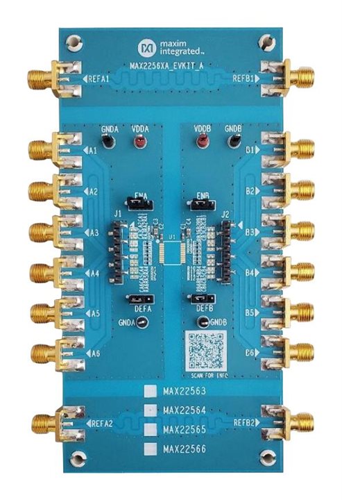 The evaluation board supports the 20-pin SSOP package type only. The MAX22163−MAX22166 and MAX22663−MAX22666 are functionally equivalent to MAX22563−MAX22566, but in different package types. The MAX22163−MAX22166 come in a 16-pin QSOP and MAX22663−MAX22666 in a 16-pin wide SOIC package.
The EV kit can be used to evaluate the functionality and electrical performance of the entire family of the devices. The EV kits should be powered from two independent isolated power supplies with nominal output voltage in the range from 1.71V to 5.5V. To evaluate the electrical parameters of the device without any isolation between the two sides, a single power supply can also be used.
Applicable Parts
Eval Kit Variants
MAX22565CAEVKIT#
MAX2256XAEVKIT#
You can also test it more in depth with your review spanning, signal integrity, power integrity, noise coupling and high voltage testing. The main features that should be called out are as follows:
CMTI = 50kV/us
| Begin Enrollment: | Dec 13, 2023 |
| End Enrollment: | Jan 18, 2024 |
| Select Roadtesters: | Jan 31, 2024 |
| Ship Unit: | FEb 26 2024 |
| Begin Roadtesting: | Mar 4 2024 |
| Element14 Follow Up: | Apr 4 2024 |
| Post Reviews By: | May 4 2024 |

Analog Devices Inc. (NASDAQ: ADI) is a global semiconductor leader that bridges the physical and digital worlds to enable breakthroughs at the Intelligent Edge. ADI combines analog, digital, and software technologies into solutions that help drive advancements in digitized factories, mobility, and digital healthcare, combat climate change, and reliably connect humans and the world. With revenue of more than $12 billion in FY23 and approximately 26,000 people globally working alongside 125,000 global customers, ADI ensures today’s innovators stay Ahead of What’s Possible.
Please see the attached PDF below for the Terms and Conditions.