RoadTest: Summer of FPGAs -- Lattice Certus-NX Versa Eval Bd
Author: dimiterk
Creation date:
Evaluation Type: Development Boards & Tools
Did you receive all parts the manufacturer stated would be included in the package?: True
What other parts do you consider comparable to this product?: Any FPGA board with 40K LUTs and above.
What were the biggest problems encountered?: Camera modules were not included , PCIe reference design is not ready for use on Ubuntu 20.02, JTAG is not always reliable , requires reboot, Very few IP cores (ex SPI master missing)
Detailed Review:
This roadtest will take a look at the Lattice Certus-NX FPGA Versa evaluation board. Many thank to Element14 and @rscansy for proving the Certus-NX hardware for this review. The plan is to test the Radiant and Lattice Propel SOC IDEs as well as test the PCIe interface of this board.
The Versa evaluation board comes with a 2 lane PCIE edge connector, a multi-adapter power supply and a USB mini cable.
The board sports two connectors for a parallel and a MIPI camera however no cameras come with the development board and most importantly no specific camera modules are specified in the documentation. As an aside I tried to use an OV5640 camera with an SMD connector for the parallel camera interface however the kit uses a different pitch SMD connector so it was not possible to mount the camera.

The kit comes with :
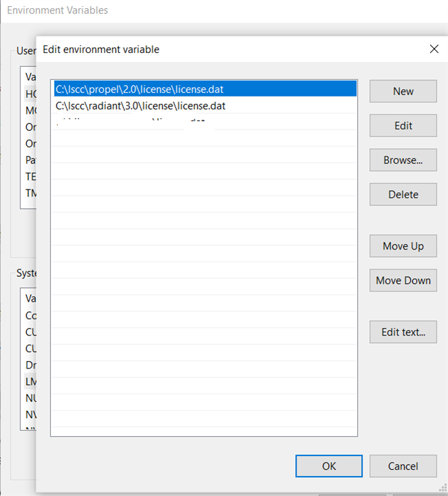
The Lattice Radiant version 3.0 , Lattice Propel and Lattice Propel builder were installed for this review. Both Radiant and Lattice Propel require a license tied to the MAC address.
Once you provide the MAC , Lattice will email you a license file. Add the License Path to the environmental variables as below and you can get started with the EVB.
Lattice Radiant is used for the RTL flow. Creating a project requires selecting the proper device which in this case is the LFD2NX family, LFD2NX-40 device in a 256 CSB package. The first project will be the obligatory blinking LED project using the 8 onboard LEDs.

| {gallery}Lattice Radiant |
|---|
|
Fig 2. Project name |
|
Fig 3. Adding HDL sources |
|
Fig 3. Selecting the FPGA chip |
|
Fig 4. Select the synthesis tool |
|
Fig 5. Finalize the project flow |
|
Fig 6. Configure PLL |
All the unused LED has to be set HIGH otherwise they will dimly light up souring current. The code below takes the 12MHz input clock from pin G13 and scales it to light up two LED’s at different frequencies.
module LEDblink(CLK_12, o_led);
input CLK_12;     // clock typically from 10MHz to 50MHz

output o_led[7:0];

// create a binary counter
reg [31:0] cnt;
always @(posedge CLK_12)
	begin
		cnt <= cnt+1;
	end


assign o_led[0] = cnt[22];    // blink the LED at a few Hz (using the 23th bit of the counter, use a different bit to modify the blinking rate)
assign o_led[1] = 1;
assign o_led[2] = 1;
assign o_led[3] = 1;
assign o_led[4] = 1;
assign o_led[5] = 1;
assign o_led[6] = 1;
assign o_led[7] = cnt[20];

endmodule
The synthesis constraints are specified on the pre-synthesis constraint files .sdc file.
create_clock -name {clk_12Mhz} -period 83 -waveform {0 4} [get_ports CLK_12]
ldc_set_port -iobuf {IO_TYPE=LVCMOS18} [get_ports CLK_12]
ldc_set_location -site {G13} [get_ports CLK_12]


ldc_set_location -site {B3} [get_ports {o_led[0]}]
ldc_set_location -site {A2} [get_ports {o_led[1]}]
ldc_set_location -site {H16} [get_ports {o_led[2]}]
ldc_set_location -site {B2} [get_ports {o_led[3]}]
ldc_set_location -site {H15} [get_ports {o_led[4]}]
ldc_set_location -site {H14} [get_ports {o_led[5]}]
ldc_set_location -site {H12} [get_ports {o_led[6]}]
ldc_set_location -site {J15} [get_ports {o_led[7]}]


ldc_set_location -site {E16} [get_ports {i_dipsw[1]}]
ldc_set_location -site {L10} [get_ports {i_dipsw[0]}]
ldc_set_location -site {L11} [get_ports {i_dipsw[2]}]
ldc_set_location -site {R3} [get_ports {i_dipsw[3]}]

ldc_set_port -iobuf {PULLMODE=UP IO_TYPE=LVCMOS15} [get_ports {switch}]
ldc_set_port -iobuf {PULLMODE=UP IO_TYPE=LVCMOS18} [get_ports {i_dipsw[1]}]
ldc_set_port -iobuf {PULLMODE=UP IO_TYPE=LVCMOS15} [get_ports {i_dipsw[2]}]
ldc_set_port -iobuf {PULLMODE=UP IO_TYPE=LVCMOS15} [get_ports {i_dipsw[3]}]
Next example will instantiate a PLL clocking IP that uses the 25MHz clock on pin F16 to generate the same 12 MHz clock as input to the blinking LED module.
The code below shows how to generate the PLL using the 25MHz clock. The fractional divider needs to be enabled to allow the PPL to generate lower clock frequencies from the 25MHz clock that meet the output tolerance.
module LEDblink(CLK_25, o_led);
input CLK_25;     // clock typically from 10MHz to 50MHz
output o_led[7:0];


// Inputs
    reg clki_i;
    //reg rstn_i;
    reg refdetreset;


// Outputs
    wire clkop_o;
    wire lock_o;
    wire refdetlos;


// Bidirs


// Instantiate the UUT
// Please check and add your parameters manually
    Clock25MHz VGAclk (
        .clki_i(CLK_25),
        .rstn_i(1),
        .refdetreset(refdetreset),
        .clkop_o(clkop_o),
        .lock_o(lock_o),
        .refdetlos(refdetlos)
        );


// create a binary counter
reg [31:0] cnt;
always @(posedge clkop_o)
	begin
		cnt <= cnt+1;
	end


assign o_led[0] = cnt[22];    // blink the LED at a few Hz (using the 23th bit of the counter, use a different bit to modify the blinking rate)
assign o_led[1] = 1;
assign o_led[2] = 1;
assign o_led[3] = 1;
assign o_led[4] = 1;
assign o_led[5] = 1;
assign o_led[6] = 1;
assign o_led[7] = cnt[20];

endmodule
One issue that was encountered consistently with radiant is that you may have to power cycle the board to get the FTDI JTAG programmed to succeed.
Also, FTUSB1 should be used for programming as channel 0 is used for the UART pins.
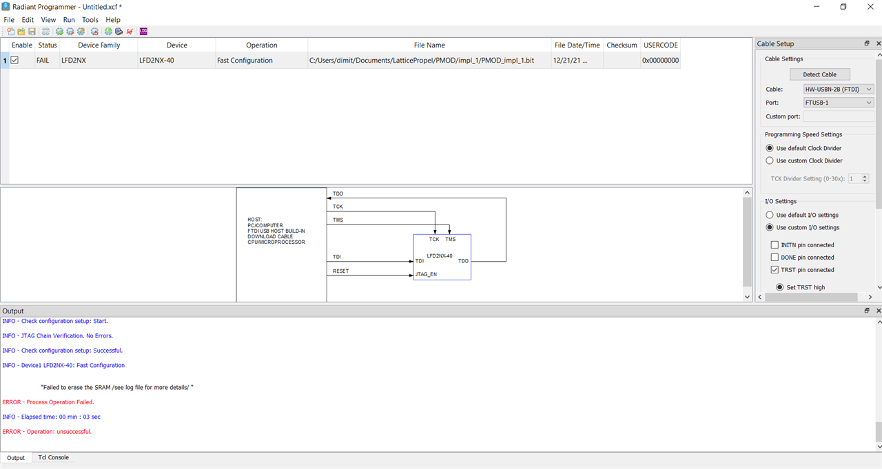
Lattice radiant also uses Lattice Reveal as an internal Logic analyzer core. I encountered timing issue during placement even for simple designs hence one needs to constrain the clocks before each synthesis run.
The board does not have any VGA connector so a VGA PMOD was added using the following constraint file on PMOD connectors J8 and J5.
create_clock -name {clk_25Mhz} -period 40 [get_ports CLK_25]
ldc_set_port -iobuf {IO_TYPE=LVCMOS33} [get_ports CLK_25]
ldc_set_location -site {F16} [get_ports CLK_25]

ldc_set_location -site {H1} [get_ports {vga_b[0]}]
ldc_set_location -site {H2} [get_ports {vga_b[1]}]
ldc_set_location -site {N1} [get_ports {vga_b[2]}]
ldc_set_location -site {K5} [get_ports {vga_b[3]}]
ldc_set_location -site {N2} [get_ports {vga_r[0]}]
ldc_set_location -site {L3} [get_ports {vga_r[1]}]
ldc_set_location -site {M3} [get_ports {vga_r[2]}]
ldc_set_location -site {L5} [get_ports {vga_r[3]}]


ldc_set_location -site {J11} [get_ports {vga_hsync}]
ldc_set_location -site {J12} [get_ports {vga_vsync}]
ldc_set_location -site {C8} [get_ports {vga_g[0]}]
ldc_set_location -site {C7} [get_ports {vga_g[1]}]
ldc_set_location -site {B7} [get_ports {vga_g[2]}]
ldc_set_location -site {A7} [get_ports {vga_g[3]}]

#ldc_set_location -site {K11} [get_ports {io_mtr_pmod0[6]}]
#ldc_set_location -site {K12} [get_ports {io_mtr_pmod0[7]}]


#UART
ldc_set_port -iobuf {IO_TYPE=LVCMOS33} [get_ports txd_o]
ldc_set_port -iobuf {IO_TYPE=LVCMOS33} [get_ports rxd_i]
ldc_set_location -site {E13} [get_ports txd_o]
ldc_set_location -site {F10} [get_ports rxd_i]
#GSRN
ldc_set_location -site {G4} [get_ports rstn_i]
#ldc_set_port -iobuf {PULLMODE=UP} [get_ports rstn_i]
ldc_set_port -iobuf {PULLMODE=UP IO_TYPE=LVCMOS18} [get_ports rstn_i]
This is still in progress as there are some timing issues that need to be resolved with the core.
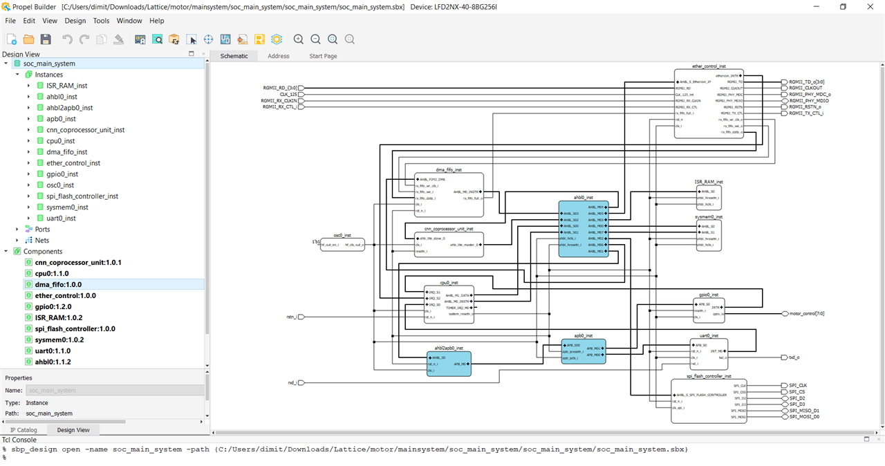
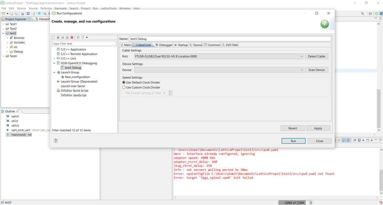
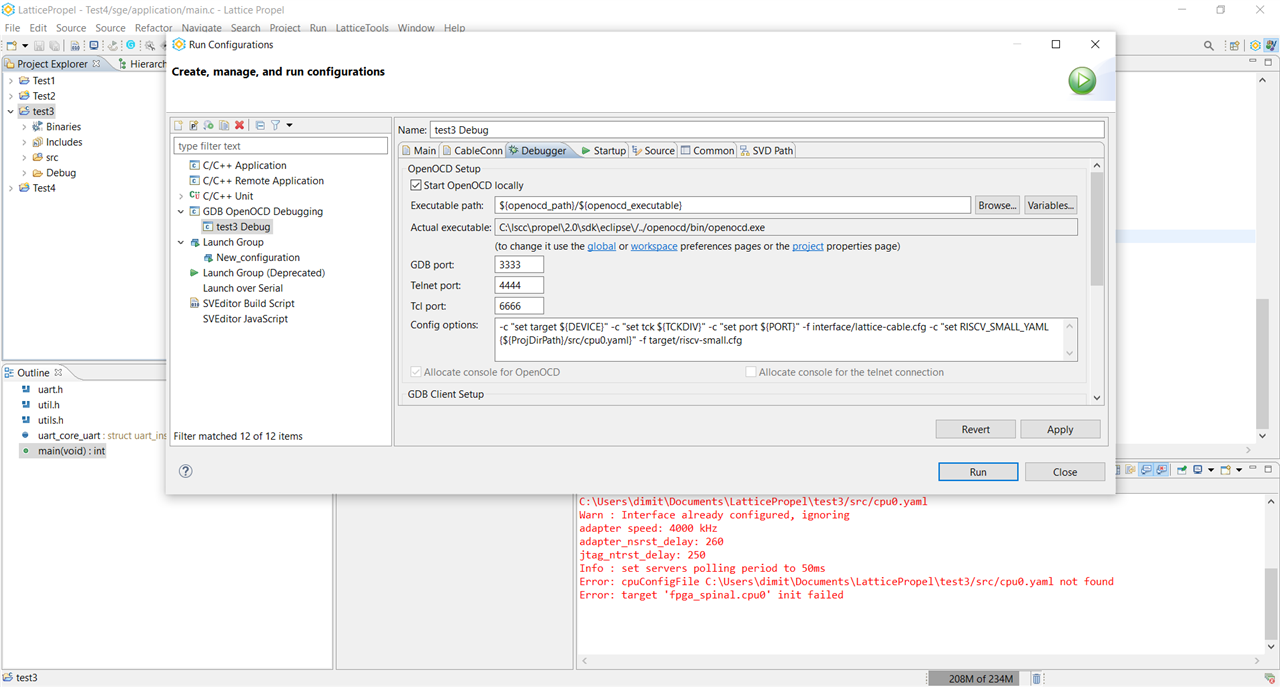
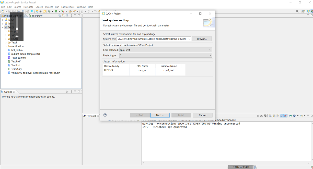
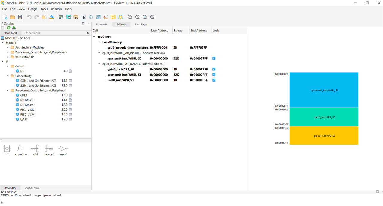
The Lattice Propel builder was used to build a RISC-V System On Chip (SOC) on the FPGA. Lattice shows two examples of this.
The first is a VexRiscv SOC with a custom CNN that makes use of TensorFlow Lite CNN accelerator to predict motor failures. The second example is a node system that also shows how to use the VexRISCV core as an MCU with custom IP cores.
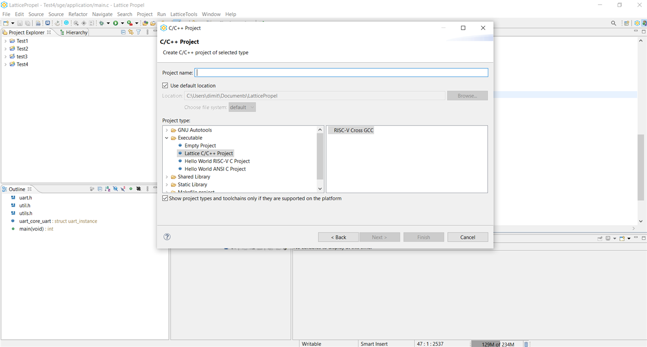
One can either design a SOC using the Block based Lattice Propel Builder and then design the firmware by importing the sbx file or simply start from the Lattice Proper Eclipse environment and create the complete system from there.

| Lattice Propel |
|---|
|
|
 |
|
|
 |
 |
 |
 |
 |
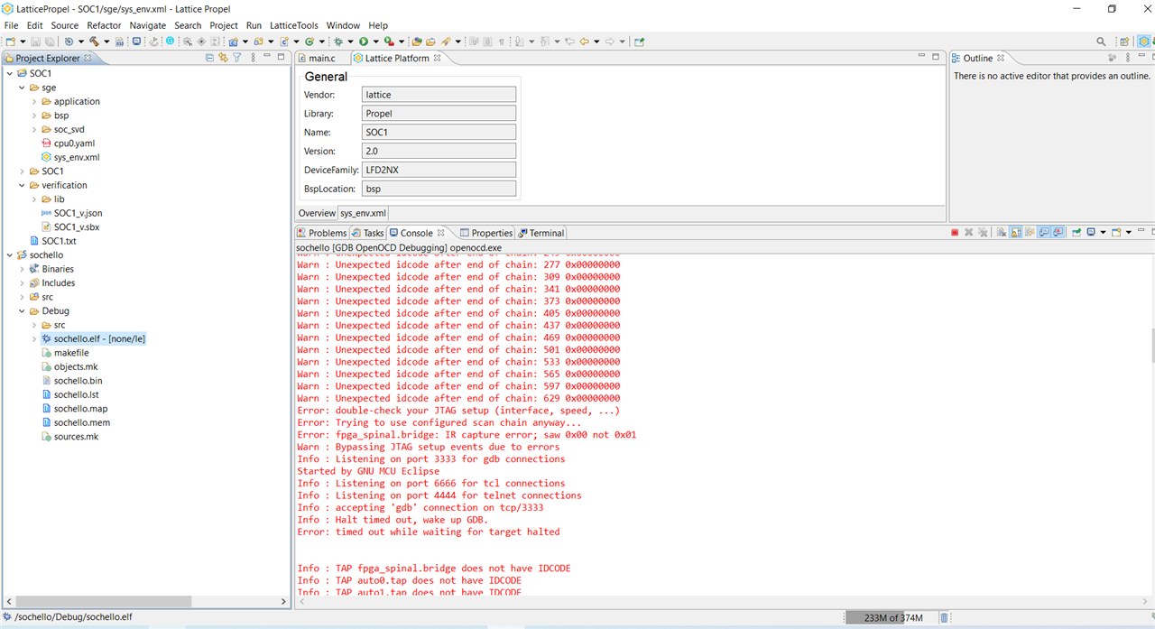 |
One issue that was encountered with these examples is that they use old IP cores of the RiscV MCU. Updating them also introduces incompatibilities.
RISCV Peripheral cores
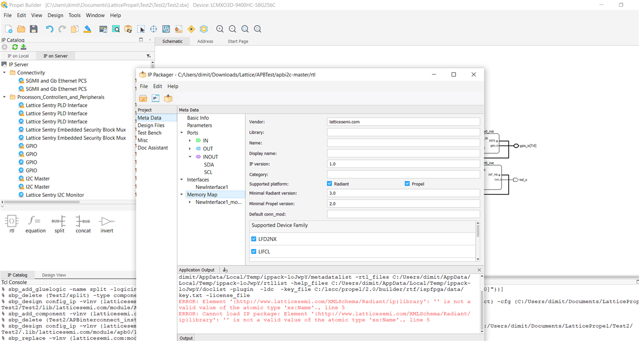
The last testing module was to build a custom APB3 IP using the Lattice provided IP builder.
Even here the flow seems straightforward but there are enough bumps that make deployment of a simple APB3 IP like an SPI master harder than it should be. Compared with Intel IP designder or Xilinx IP integrator the IP design GUI lacks the polish and gives cryptic errors.
The Versa board can be installed on a motherboard PCIe x2 slot.
Before that one has to install the PCIe kernel driver and compile the GUI. The aim is to control the 7- segment display from the desktop GUI using the PCIE as an endpoint.
To test the PCIe package run the Linux install script. The package states that the kernel module is compatible with Kernel 5.x. However upon installing this as you can see below there are compilation errors that preclude the installation of the kernel module.
| {gallery}PCIE test |
|---|
|
PCIE kernel driver installation issue |
|
Kernel compilation issue |
|
GUI |
|
GUI |
|
GUI |
|
GUI |
To test the PCIE the bitstream has to be programmed first. After installing one can query the board using lspci command.
However not much can be done without a working kernel module.
The PCIe package was released in November and as of December 27 it has been removed from the Certus-NX Versa evaluation board page again so it may be updated in the near future again.
Verdict
The Good
1. 40K LUT FPGA with PCIE connector and 1G Ethernet
2. Radiant supports scripted tcl flow
The Bad
1. PCIE kernel module cannot compile on Ubuntu 20.02
2. No camera modules or references for specified connectors
3. Lattice Propel Vexrisc core has a very limited number of IP cores (no SPI master)
4. MIPI DPHY core not available for free
5. GUI English translation (specifically errors) are lacking so Lattice Radiant may require some further polishing