RoadTest: Summer of FPGAs -- Lattice Certus-NX Versa Eval Bd
Author: kvik86
Creation date:
Evaluation Type: Development Boards & Tools
Did you receive all parts the manufacturer stated would be included in the package?: True
What other parts do you consider comparable to this product?: Xilinx, Intel boards
What were the biggest problems encountered?: More example projects are needed.
Detailed Review:
This roadtest deals with the Certus-NX Versa Evaluation board from Lattice. The board is build around the Lattice Certus-NX-40, 256 pin BGA FPGA, specifically the LFD2NX-40 8BG256CES variant. The board contains a DDR3 memory chip, SPI flash for storing the configuration bitstream, two gigabit Ethernet interfaces, PCIe connector, two camera connectors, DIP switches, buttons, a seven segment display, some signal connectors, and an FTDI chip for USB JTAG programming.

Top view of the board
The development board is really useful to get started with interfacing such components (gigabit ethernet, DDR3 RAM, PCIe, MIPI, parallel camera interface). As most of them use high-speed interfaces, it is really beneficial to know that the board layout is ready and usable, prototyping, which can be expensive and also prone to errors, becomes much easier.
The board is powered by a 12V adaptor, except when it is placed in a PCIe slot. Programming and debugging can be done using the FTDI USB chip on the board.
The Certus-NX devices are categorized as low power, general purpose FPGAs by the manufacturer. These devices are part of the Nexus platform from Lattice (Crosslink-NX, Certus-NX and CertusPro-NX), which can be considered quite new, debuted recently in 2020.
Products from Lattice
There are two main versions of the silicon, a smaller one containing 17k logic cells (LFD2NX-17) and a bigger one with 39k logic cells (LFD2NX-40). There are also differences in the number of embedded memory blocks (24 vs 84 x 18kb), number of multipliers (24 vs 56), distributed RAM size (80 vs 240kb), large RAM size (2560 vs 1024kb). The larger device contains more PLLs and contains hard PCIe Gen2 interface. Both contain a cryptographic engine supporting true random number generator, hash algorithms, ECDSA signature generation etc. Each device is available in different packaging and at different speed grades. Naturally only in BGA packaging. The price right now for such a devices is around 30-60 USD depending on the number of logic cells and IOs.
Compared to simpler devices from the manufacturer, such as the MachXO2-3 devices, the Certus-NX line offers more logic cells, more memory (even large memory blocks), contains hardware multipliers, ADS blocks and supports faster interfaces (PCIe, DDR3, GMII).
The CertusPro-NX family is even more capable, providing 50k or 100k logic cells, more multipliers, more RAM, IO, supporting 10GbE, PCIe Gen3, LPDDR4 and so on.
The Certus-NX devices are capable enough to implement softcore processors while also providing enough logic cells to implement additional custom logic.
These devices do not have embedded flash, so an external memory chip is needed to store configuration data.
Useful links:
The board arrives with a miniUSB cable and a 12V adaptor. There are plenty of functional and current measurement jumpers on the board, fortunately they were preinstalled.
The schematics of the board and signal descriptions for the connectors can be found in the user’s manual, see the useful links section. Unfortunately, gerber files (or other pcb source projects) are not available so one needs to follow traces (which ones are length matched?), do some measurements, debugging not directly on a connector, it might be difficult.
The first page of the schematics is a table of contents, the second provides an overview about what dives are connected to which banks of the FPGA. The third page shows the FTDI USB chip (FT2232H). The A port is used as JTAG, B port can be used as UART (TX and RX only) or I2C. By default, TX and RX jumpers are closed. Transmit and receive directions are from the point of view of the PC (FTDI to the FPGA), not the FPGA. There is an I2C EEPROM that contains the configuration for the USB chip. This can be reprogrammed by the FT_PROG utility from FTDI. This is needed to change the interfaces such as from UART to I2C. The board contains a header that can be used to program other devices using JTAG.
The next page contains the schematics for Bank0, which is mainly used for configuration (INITN, PROGRAMN, DONE signals, QSPI flash). The DIP switch is also placed here, but only DIP_SW2 signal is connected to Bank0. The two ADC ports of the FPGA with voltage reference and supply is also populated here.
The fifth page shows how JTAG, UART, I2C and the seven segment display is connected to Bank1. Multiple clocks are also connected here: DDR3_CLK, 12MHz, 25MHz, 27MHz. 25 and 27MHz oscillators are also shown on this page.
The next page details Bank2, the LEDs, PMOD0 and PMOD1 headers are connected here. A 100MHz and a 125MHz oscillators are instanced here and are also connected to Bank2.
Page 7 shows Banks 3 and 4. DDR3 memory and the MIPI camera are connected here. According to the schematics, the DDR3 chip is model MT41K64M16TW-107 (128MB, 1Gb). Not sure if the camera interface and the memory can be used at the same time, the schematics notes 1.5V for the DDR3 memory and 1.2V for the D-PHY interface. Fortunately, the signals are not overlapping.
Page 8 shows Bank5 and the SGMII (DP83867ERGZT chip) Ethernet interface. The next page shows the other Ethernet port using RGMII interface with the DP83867IRPAPR chip and the header PMOD2.
Page 10 details Bank7 and the parallel camera connector (not sure which was assumed to be used here), pushbuttons and an integrated LDO with 3 output voltages for the camera. Page 11 shows switched mode power supplies for 1.2V, 2.8V, 1.8V and 1.05V and the MIPI camera connector. Unfortunately, this pinout looks different from the one used with the “standard” IMX219 camera (and one of the voltages: 1.05V differs from the 1.2V used on the Sony camera). According to the BOM, the Sony IMX214 pinout was used.
Page 12 shows the PCIe interface. Page 13 contains power selecting jumpers: J47, J16, J48 etc. Some port supply voltages can be configured by these jumpers. Page 14 contains power pins and decoupling capacitors for the FPGA. Page 15 is packed with power regulators for the FPGA, camera, GbE PHYs, DDR3 memory, PCIe etc. Finally, page 16 contains a block diagram of the power delivery, the supply voltages used by different devices on the board.
Useful links:
There is a sample project that can be downloaded from the manufacturer for demonstrational purposes for this board. This demo uses the PCIe interface to communicate between the PC and the FPGA. Two functions are demonstrated: a simple demo allows us to control the seven segment display on the board from a PC application, and there is a bandwidth demo that allows the PC to access (read and write) memory in the FPGA. This latter one is a really useful starting point for developing other applications.
I tested the demo on Windows, however a Linux version of the driver and demo app is available as well.
First I checked all the jumpers on the board according to the manual. According to the manual they should be set up correctly in the factory. The was some disturbance in the Force, according to the quick start guide, J47 should be in the 1-2 position (as it was), however the detailed guide showed position 2-3 for J47. This jumper selects 1.8V (1-2) or 3.3V (2-3) for VCCIO0, which is also used to power the SPI flash containing the FPGA configuration. According to the docs the flash chip should be MT25QU128ABA1ESE-0SIT from Micron, which supports 1.7-2.0V supply. I could not confirm the exact product number by looking at the markings. So, I voted for the 1.8V position, leaving the jumper as it was.
I connected the 12V power supply to the board, no smoke, Christmas-tree lights, good sign. Next, I opened up Radiant and the programmer module, and tried to read back the configuration from the flash, just in case, however I got chip ID reading errors. I couldn’t flash the chip as well. Finally I gave in and set the VCCIO0 to 3.3V, and miracle, it worked right away, I could read back the factory config and I could also download the one provided for the demo. Fortunately, they were exactly the same, byte-ot-byte. After flashing, I reset the VCCIO0 to 1.8V again, to see what happens. As the DONE (configuration) LED lit up, I suppose the flash did work, but not sure why 3.3V was needed to access it through Radiant. Especially as 3.3V is out of its recommended (allowed) supply voltage range.
Next, I installed the demo software for Windows (10), but the driver install failed as it was not signed (as anticipated). Restarting using the advanced boot menu did the trick. I was surprised that it turned out this was not only needed to install the driver but to use it as well.
The driver loaded, demo software detected the FPGA, controlling the seven segment display worked without any problems. So did the memory reading and writing.
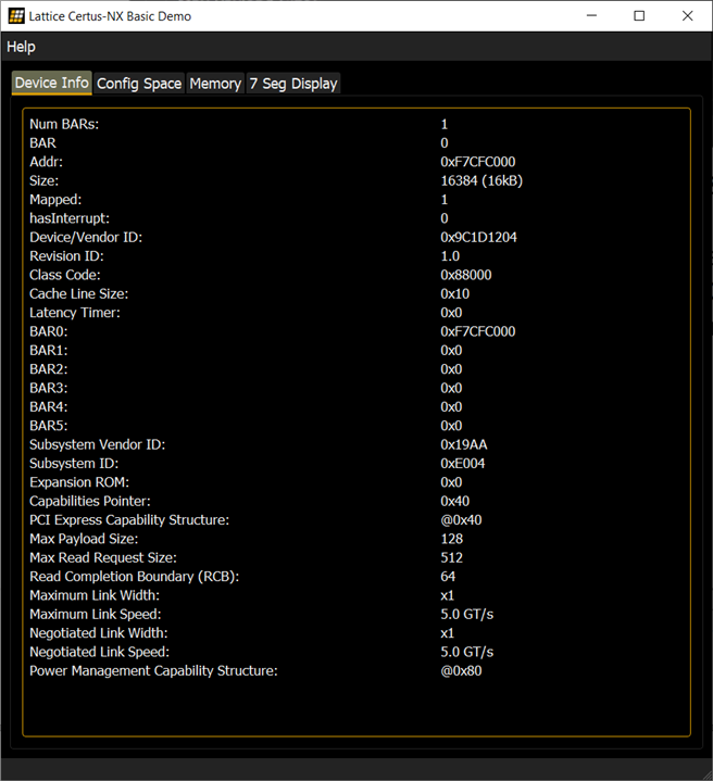
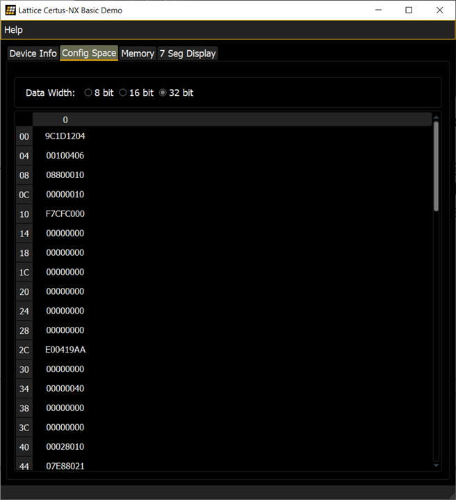
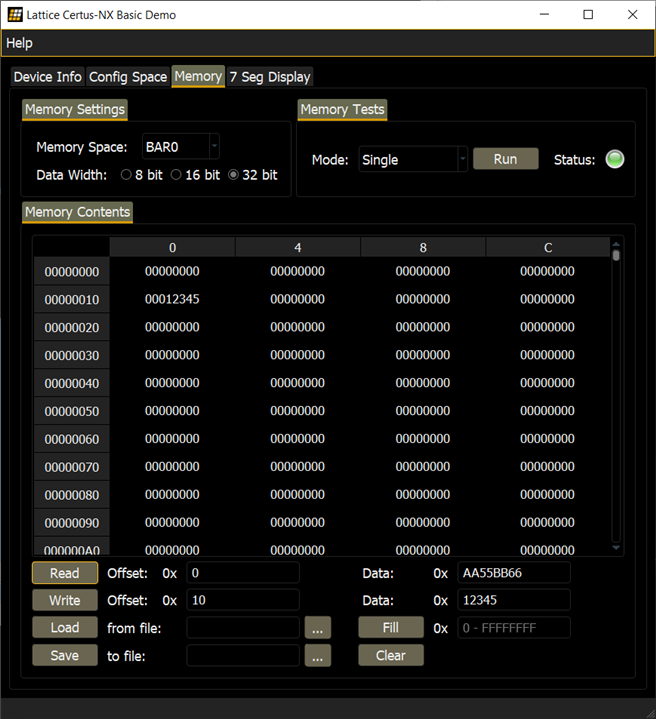
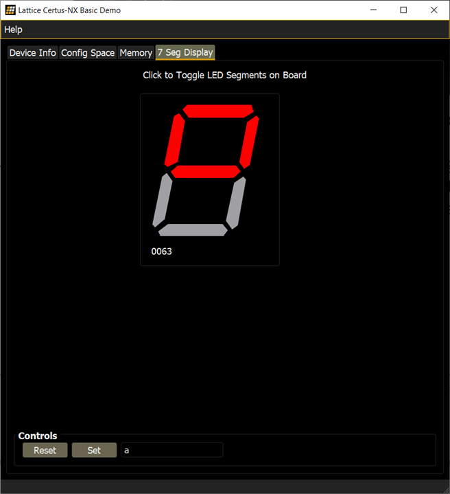
Screens from the test application
The demo code also contained a library besides the client application and the driver. It is a C library with a very simple interface for reading and writing data from/to the FPGA. I have Visual Studio and VS Code installed, but after a few hours I couldn’t get the linking with the static library working well (although I did similar many times before), so I moved to testing it using the dynamic library (not very nice…). I’m sure it is possible, but I might have missed a compiler or linker setting.
I used LoadLibraryA() and GetProcAddress() to load the .dll and get the function pointers for the specific exported functions.
#include <stdint.h>
#include <windows.h>
#include "Ioctl.h"
#include "MemRwApis.h"
#include <iostream>

typedef int8_t(*open_drv_t)();
typedef int8_t(*close_drv_t)();
typedef int8_t(*getPciResources_t)(PCIResourceInfo_t* PCIinfo);
typedef int8_t(*read32_t)(uint32_t addr, uint32_t* data);
typedef int8_t(*write32_t)(uint32_t addr, uint32_t data);

int main()
{
    std::cout << "Hello World!\n";
    PCIResourceInfo_t info;
    int8_t err;
    HMODULE lib=LoadLibraryA("MemRwApis.dll");
    if (lib == NULL) { return -1; }

    open_drv_t open_drv =(open_drv_t)GetProcAddress(lib, "open_drv");
    close_drv_t close_drv = (close_drv_t)GetProcAddress(lib, "close_drv");
    getPciResources_t getPciResources = (getPciResources_t)GetProcAddress(lib, "getPciResources");
    read32_t read32 = (read32_t)GetProcAddress(lib, "read32");
    write32_t write32 = (write32_t)GetProcAddress(lib, "write32");

    err= open_drv();
    getPciResources(&info);

    uint32_t rwaddr=0x0;
    uint32_t wdata = 0xaa55bb66;
    write32(rwaddr, wdata);
    uint32_t rdata;
    read32(rwaddr, &rdata);

    close_drv();

     return 0;
}
Fortunately, it worked right away and I could also see the changes in the demo client application.
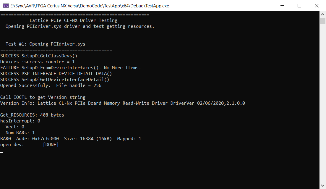
Using the demo communication library
The sample PCIe project (for the FPGA) is available as source, which is a great start if someone wants to start an application with PCIe connectivity.
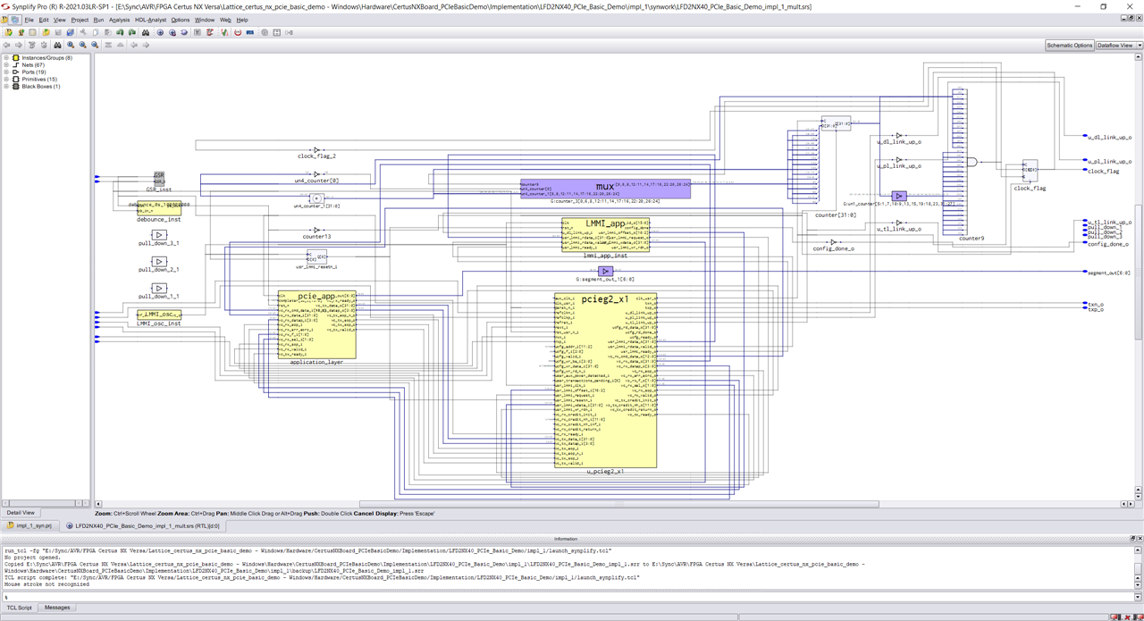
Sample PCIe project hierarchy view
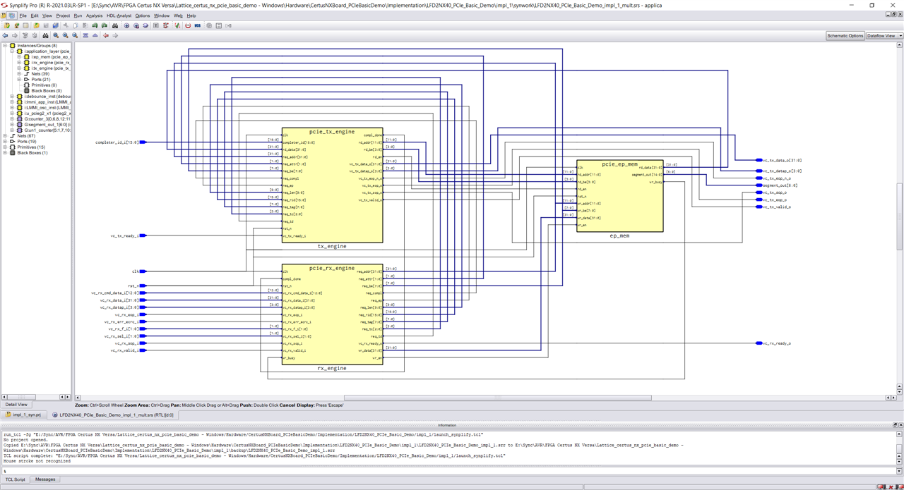
The sample PCIe project application logic hierarchy view
The evaluation board contains a DDR3 memory chip (MT41K64M16TW-107). These memories offer large capacity and high bandwidth, however the latency is not negligible, the state machine and the controller is complicated. Also, the number of signals and traces needed to connect the memory and the FPGA is quite large. DDR3 memories use dual data rate, meaning data is transferred both on the rising and falling edges of the clock signal. Such memories, in order to increase bandwidth, have a slower internal clock and a faster IO clock, and they operate in a 8n-prefetch mode, meaning in every internal clock cycle 8 bits are accessed and these 8 bits are transferred in 4 IO clock cycles (8 half clock cycles).
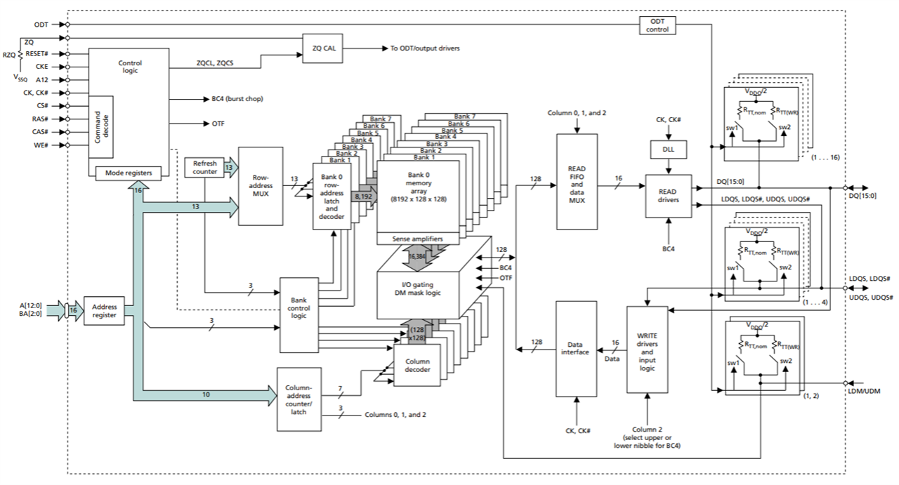
DDR3 memory block diagram (from datasheet)
The memory is organized into (8) banks, each bank having a number of rows (8192) and columns (128) consisting of a number of bits (128). Each 128 bits of data is transferred in 4 cycles on the external 16bit wide bus. Banks operate independently, different instructions can be sent to banks, however due to only one IO bus, only one can do reads or writes at the same time. Other commands may overlap and also due to latencies, the external bas can be utilized quite efficiently. In order to access a row in a bank (read or write), the row must be activated, when the operations are done, it must be deactivated (precharge instruction). Only one row can be active in a bank. Periodically a refresh instruction must be executed on each row in order not to lose the stored data. Refresh can be done manually or automatically. At startup, a configuration sequency must be done to initialize the memory chip.
Lattice provides a DDR3 controller IP for Certus-NX and Radiant, supporting all sorts of memory configuration (8-32 bits wide data bus, burst lengths, latency configuration, refreshing etc.) through a native interface. Still, it takes some effort to get the memory up and running through this interface from custom HDL code. Unfortunately, I didn’t find the DDR3 IP in Propel Builder, which would make a lot of sense to use the external memory with a softprocessor. Perhaps an DDR3 Native interface to AHB bus module is required. Hopefully this will become available as the platform is pretty new. A big bummer is that this IP requires a license to be utilized fully and it is quite expensive (ok, it depends… around 1700$+). Evaluation is possible, not only using simulation but in hardware as well, however it is supposed to run only for a limited time: about 4 hours.
Something similar is going on with the Ethernet interfaces as well. There is an IP available (again, 1700$+), can be evaluated in hardware as well. There is an SGMII and Gb Ethernet PCS IP in Propel Builder, however it seems to be not using AMBA bus, so it does not seem to be simple to connect to the softcore processor.
This is a bummer, I hoped to get something really interesting working, the hardware is available, but software seems to be lacking behind.
The Diamond IDE is succeeded by the newer Lattice Radiant. The interface is nicer, but most of the features are the same.
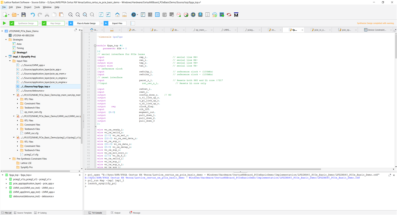
Lattice Radiant code editor
The File List tab at the left side contains the project tree. Here we can find the selected device, synthetization strategies (settings), all the input source files, debugging, programming and other files. At the bottom, the hierarchy of the modules is also shown. The next tab, Source Templates contains different code templates, such as Verilog or VHDL snippets and different primitives provided by the FPGAs to instantiate. The third, IP Catalog tab provides configuration and instantiation of complex modules: DSP based modules, different RAMs, ADC or IPs that are in the catalog online or that are installed from file. The IP on Server tab shows the IPs provided by Lattice.
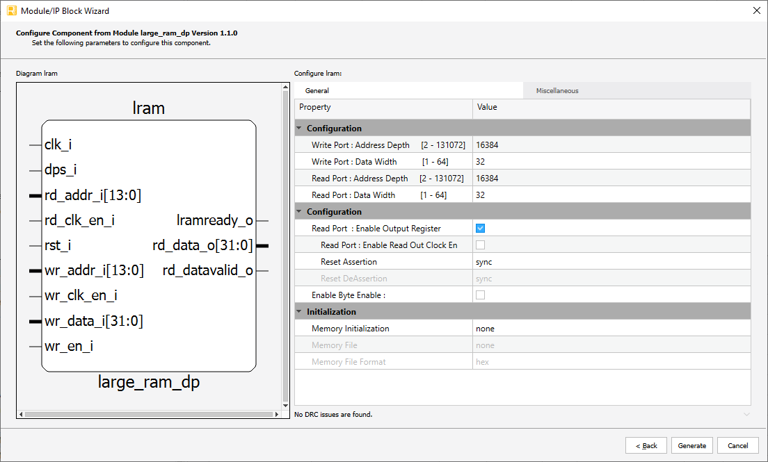
Example memory instantiation (Large RAM)
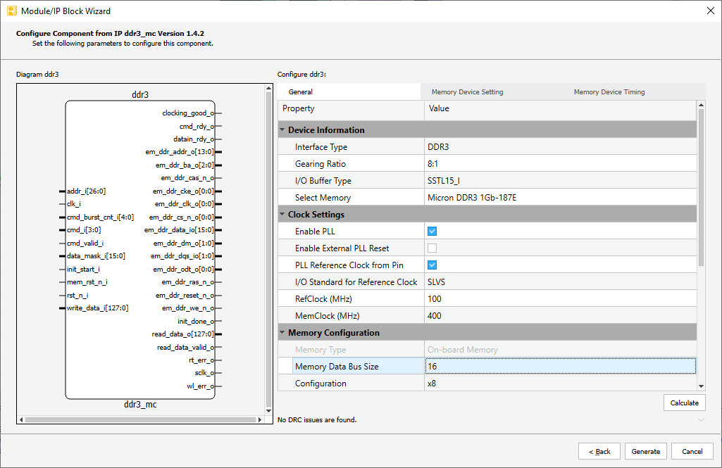
Example DDR3 controller IP instantiation
The toolbar on the top can be used to run steps of the synthesis process. There is also a dropdown to specify which substeps (such as timing analysis) to do or ignore. This looks nice, as it is always visible and takes less space than in Diamond.
The Tools menu is also very similar, however the “Spreadsheet” was changed to Device Constraint Editor. This tool is probably the most important, it is used to connect internal nets to pins of the device and also configure the IOs: specify the IO type, enable differential 100R resistor, open drain mode, set pull mode, slew rate, hysteresis etc. A device view is also provided to provide visually feedback about the layout of the pins. The global tab specifies other general configuration for the device: Enable or disable default ports (SPI, I2C, JTAG etc.)
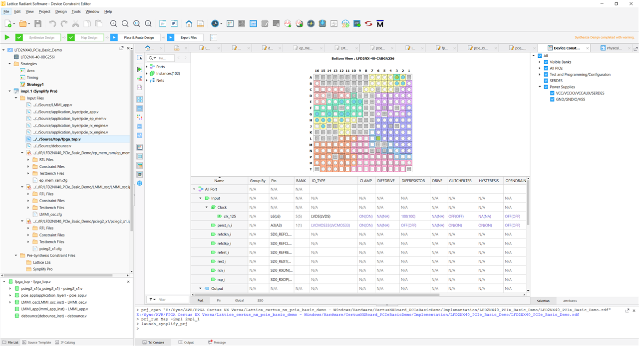
Pin assignment screen
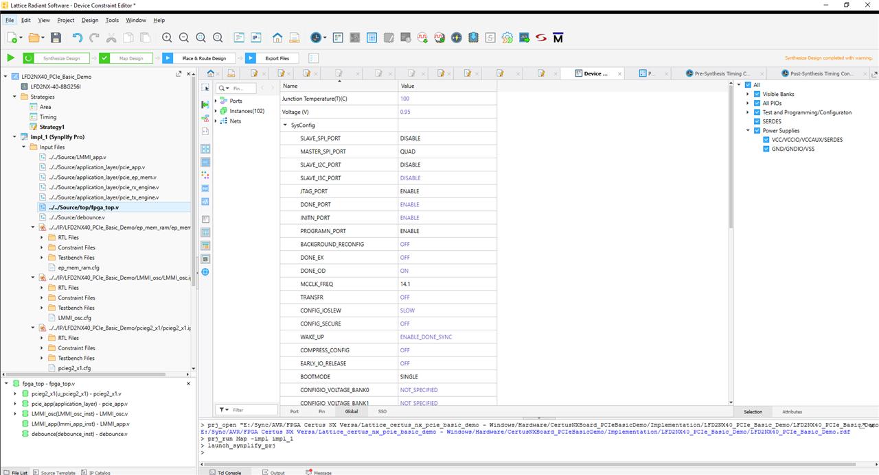
Device constraints, configuration spreadsheet
Timing Constraints Editor allows us to define operating frequencies for different clock signals, allowing the synthesizer to find layouts that satisfy these conditions (hopefully). This was previously part of the “Spreadsheet” tool, but I believe it is more useful this way.
Timing Analyzer tool is enabled if multiple steps of the synthesizer has run and the timing analysis substeps were enabled.
If Synplify Pro was selected as the synthesis engine (the other option is Lattice Synthesis Engine), Synplify Pro for Lattice opens the Synplify tool, which allows to browse, look at the modules, the connections, see all sorts of debug information about timings, resource usage, configure the compiler etc. ModelSim can be used for simulation, it installs with Radiant.
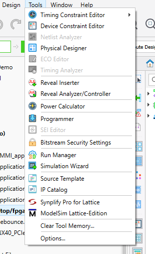
Radiant tools menu
I started a black new project to test the features and the board from scratch. I created a simple topmodule with a 32 bit counter and set the top 8 bits to LED outputs. The clock was an external 125MHz clock input. I set the pins for the device constraints according to the schematics. After the synthetization completed, I used the Programmer tool to copy the configuration to the SRAM. Fortunately, the LEDs started blinking just the way they were intended to.
Next, I tested Reveal, the embedded logic analyzer. I used Reveal Inserter to select which signals to sample, specify the number of samples to collect. Trigger was also set to a rising edge of an LED out. After synthesis and programming completed, I opened Reveal Analyzer/Controller tool. Here the device had to be selected (USB/JTAG device, reveal descriptor) and scanning found the reveal-capable device. Sampling and triggering completed successfully, however manual trigger is also available, which is pretty useful. The counter bits showed up nicely.

Reveal setup for the counter test
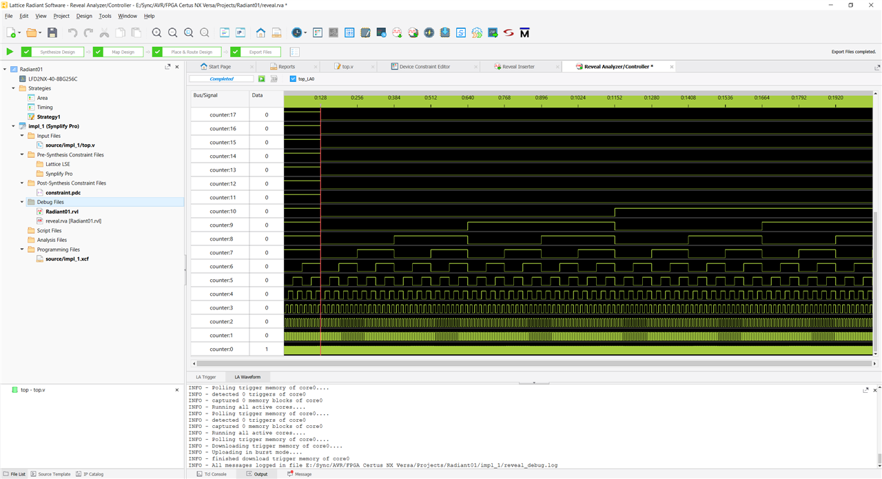
Reveal showing nice counter bits
Useful links:
Propel Builder provides a GUI for module instantiation and configuration. By default, it comes with RISC-V softprocessor cores (RISC-V SM and MC), different AMB bus interconnects (AHB, AHB to APB, APB), basic peripheries (GPIO, UART, I2C, Timer-counter) and other IPs. More IPs can be downloaded from the repository, however I wish there would be even more. Much more.
Architecture modules can also be instantiated, such as the on-chip oscillator, PLL, different memories, arithmetic modules.
Custom IPs packages can also be created using the Tools->IP Packager menu item.
Not only packaged IPs can be instantiated and connected, but simple logic expressions, gates, HDL source modules (glue logic) can be added. Modules sources can be given at instantiation of source files can also be selected. Custom modules, peripheries implementing the APB or AHB bus can be relatively easily be added to the system.
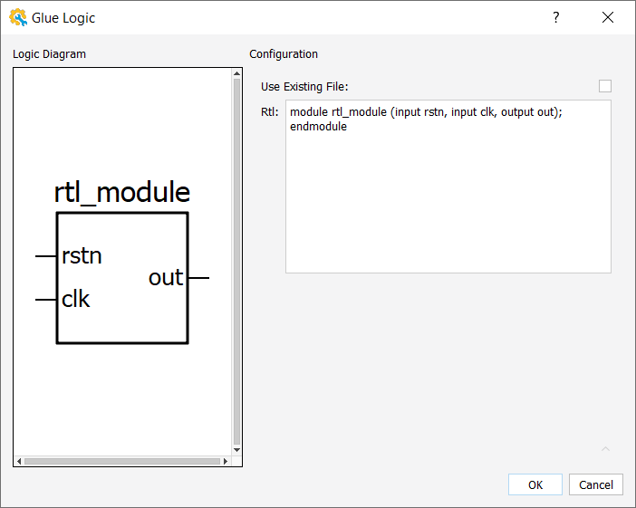
Custom glue logic insertation, the schematic symbol updates as the code updates
I started with the Hello World template. It contains the internal oscillator as a clock source (112.5MHz). This is fed into a PLL, which bypasses the input clock for the CPU and the AHB bus, but creates a quarter frequency (28.125MHz) for the slower APB bus. The system contains a RISC-V MC processor (this is the more complex one compared to the RISC-V SM). The instruction bus is connected directly to the main system memory module, while the data bus is through an interconnect. The main memory module wraps EBR primitives as RAM and it also contains the code. After the code is compiled in Lattice Propel for this system, the code memory image can be set for the main memory, thus the generated system will contain and run the RISC-V code. An AHB2APB bus is connected to the AHB interconnect, the APB bus contains an APB interconnect that allows two APB peripheries (GPIO, UART) to be connected to the system. As the peripheries implement the AMBA APB bus, registers and addressing is used to access them by the processor. The address configuration can also be done, the GUI even shows a graphical representation of the reserved addresses. I encountered some cases where LMMI (Lattice Memory Mapped Interface) was (or can be) used by a periphery instead of the AMBA busses. (GPIO IP has selectable LMMI or APB interface.)
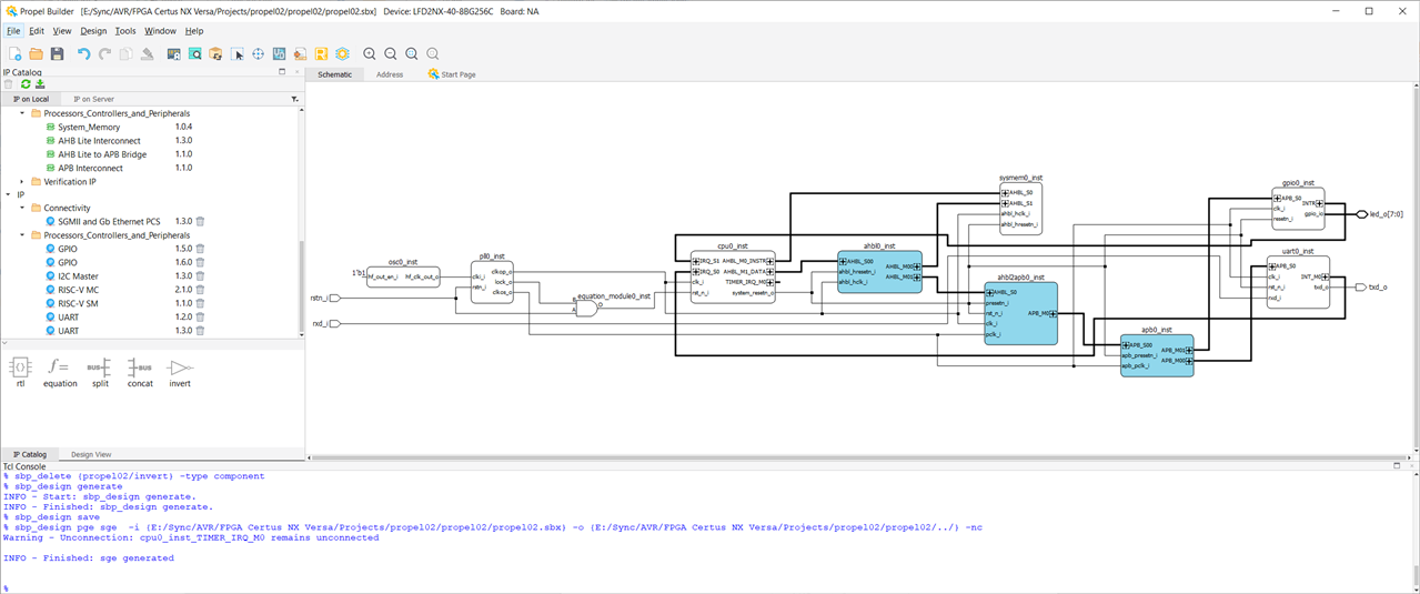
Hello world example project - RISC-V MC, RAM, GPIO, UART, internal oscillator
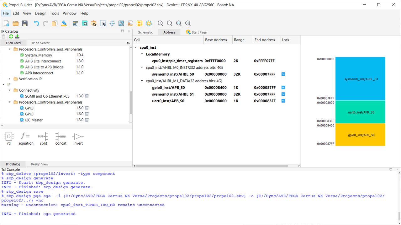
Default memory layout

Captured Hello World UART message
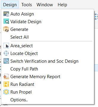
Propel Builder Design menu
Unfortunately, I haven’t found official solutions for the DDR3 memory to be used with the RISC-V core in Propel, neither the SGMII interface with the AMBA bus (nor any ethernet drivers/stack…).
Useful links:
Propel Builder opens Propel, which is an Eclipse-based C/C++ IDE. The Design->Run Propel options opens op Propel with a Wizard for generating a new project for the system. It even comes with basic driver support for the simple peripheries in the build (GPIO, UART, I2C). The hello world sample contains a chase light code for the LEDs and sends a hello world message over UART. The clock frequency symbol CPU_FREQUENCY was 90,000,000 by default, I changed it to 112,500,000 according to the settings in Propel Builder. I compiled the sample project which created a hex (not Intel HEX) memory map file, that could be loaded back to the system memory in Propel Builder. Propel Builder finally generated a Radiant project, that could be synthetized and programmed to the device. I set up an OpenOCD debugger configuration in Propel, leaving everything as default, except I selected the JTAG device and ran a scan which found the CertusNX FPGA.
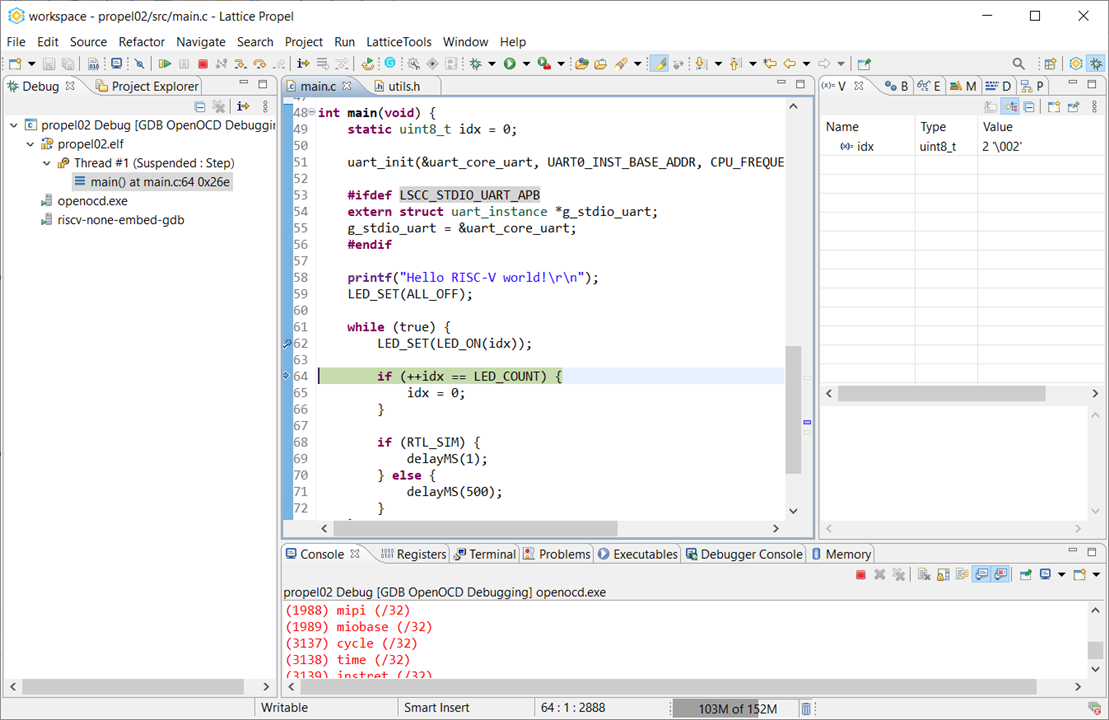
Propel live debugging the softcore RISC-V through OpenOCD
After this debugging worked, I could step execution, see variables and registers.
Changing some configuration, switching between the IDEs (Radiant, Propel, Propel Builder) sometimes resulted in strange behavior, I expect some things are not always in sync. Radiant project regeneration removed some settings, in some cases I wasn’t sure which version it actually synthetized etc. This probably could be improved.
Sometimes when programming the FPGA I got incorrect chip id error, which was resolved by powering off and on the board. Sometimes OpenOCD didn’t start, or was already started, but not stopped correctly (timeout or cableserver connection error). At some point, (perhaps when a Propel Builder project was regenerated, the constraint file was discarded?) all my pin settings were discarded, no wonder the correct outputs weren’t controlled. I just hope no output pins were killed in the process.
Finally, I managed to get Propel Builder generated project with a RISC-V softcore running C code, while debugging and using Reveal at the same to watch APB transfers.
I captured the signals for an APB write transaction when using the GPIO (setting the LEDs). The address is only 6 bits, the address range of the peripheries is 0x400. Assuming that only 4 aligned addresses are valid, it seems to be right. The APB interconnect takes care of the base address selection, the devices only get the relative address.
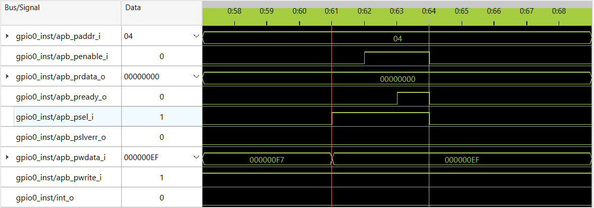
APB write transaction for GPIO periphery
The APB write is as follows, from the specification:

First in T1 (Setup phase), the Address, Select and Write is set. Address and Write didn’t change in the example as LEDs were only written and the last transaction also addressed the same periphery. Next Enable is set by the master (Access phase). Finally Ready is set to one by the periphery to signal that the transfer is over.
The feature set provided by this FPGA is pretty impressive. I like the idea that there are not tens of different types in the device family, only two (so far), and there are only a few packaging options. This provides better chance to actually be able to find the one that is needed at the distributors. The number of LUT allows softcore processors to be used realistically in these devices. LargeRAM and DSP blocks provide wider range of applications than simpler devices, such as the MachXO series. Unfortunately, but naturally such complex devices are only available in BGA packaging.
I believe the manufacturer should provide much more IPs (and for free), in order to allow the user to use the device as a configurable microcontroller, which sounds reasonable as softcore processors are a viable in these devices (which are intended for general purpose usage). GPIO, UART, I2C, SPI, basic timers are a great start, but not enough, these are the ones that require the least effort to get working.
For the development board, there should be more examples available, such as for the DDR3 memory and the gigabit Ethernet interfaces. I’d love to see some higher level interfaces, for example a SGMII controller that would take care of DHCP and some other infrastructure-related packets, and would give me an interface of IP address, port and a FIFO or addressable RAM which describes the data that would be sent as an UDP packet or received by an UDP packet. Not even talking about TCP. It should take care of the header generation etc. It seems now extremely difficult to use the Ethernet interface without a soft processor.
Somewhere I stumbled across the information that the MIPI board connector is compatible with the Sony IMX219, and I got really enthusiastic. I didn’t look into this in more details. However, as I was close to connecting my camera module and going through the schematics to be sure, I realized that the signals of the 30 pin connector is not compatible with my IMX219 and realized in the BOM list for the Versa board that the IMX214 was supposed to be used here. Unfortunately, I couldn’t get such a camera module until the deadline and also getting working I2C configurations are quite difficult, as most are not public. Even with a datasheet. As the IMX219 is the Pi v2 camera, lots of information is available about it. I’ll try to create an adapter board that connects the appropriate signals and power to get the IMX219 working.
The FPGA itself and the development tools are really great, however it feels like software (IPs, examples etc.) are lacking and I was a little bit disappointed that I couldn’t get (in the given timeframe) any of the really interesting interfaces working (DDR3, SGMII, MIPI-CSI2). However, I’m not giving up, I’ll continue to learn and try the world of FPGAs even with this board.