RoadTest: Enroll to Review the ADI Energy Harvesting EVB ADP5091-2-EVALZ
Author: Unknown
Creation date:
Evaluation Type: Evaluation Boards
Did you receive all parts the manufacturer stated would be included in the package?: True
What other parts do you consider comparable to this product?: MAX20361EVKIT#,STEVAL-ISV020V1,STEVAL-ISV019V1,EM8500,ADP5090-2-EVALZ, ADP5091-1-EVALZ
What were the biggest problems encountered?: Connector pins not labelled
Detailed Review:
Thanks for choosing me to review and evaluate the energy harvesting plug and play evaluation board, EVB ADP5091-2-EVALZ by Analog Devices.
The review is divided in eight (8) sections.
In Section 1, I will unbox boards received for this review. Then I review two boards separately.
In Section 2, I will explain one board - ADP5091-2, chosen circuits for evaluating and board connections in simple language.
In Section 3, I separately evaluate 2nd board - Alta Devices PV board.
In Section 4, the plots of performance characteristics of ADP5091-2-EVALZ are given.
In Section 5, the chosen circuits for evaluating ADP5091-2-EVALZ given in Section 2, are practically evaluated.
In Sections 6, 7 and 8, the general feedback, comparable products and conclusion is given respectively.
Table of Contents
Following are the unboxing pictures
1) Unboxing Analog Devices ADP5091-2-EVALZ
| {gallery}Unboxing Analog Devices ADP5091-2-EVALZ, 360° view |
|---|
|
IMAGE TITLE: Unboxed, All Items Together |
|
I
|
|
|
|
|
|
|
|
Printed 9 page datasheet on high quality paper with colored page of 'Evaluation Board Layout'. There are separate 28 pages which have to be referred. |
If I have to buy, I will like to see complete unbox images with 360° view and what's all inside the box. And it has country of origin : USA !
2) Component Protection Pads (for transportation)
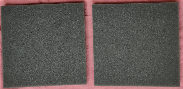
Below two pads are very soft and good to protect damage, so very good packaging, and they deserve separate photoshot!
(a) Pads One Side
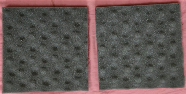
(b) Pads Back Side
3) Analog ADP5091-2 Evaluation Board
(a) Front of Analog ADP5091-2 Evaluation Board
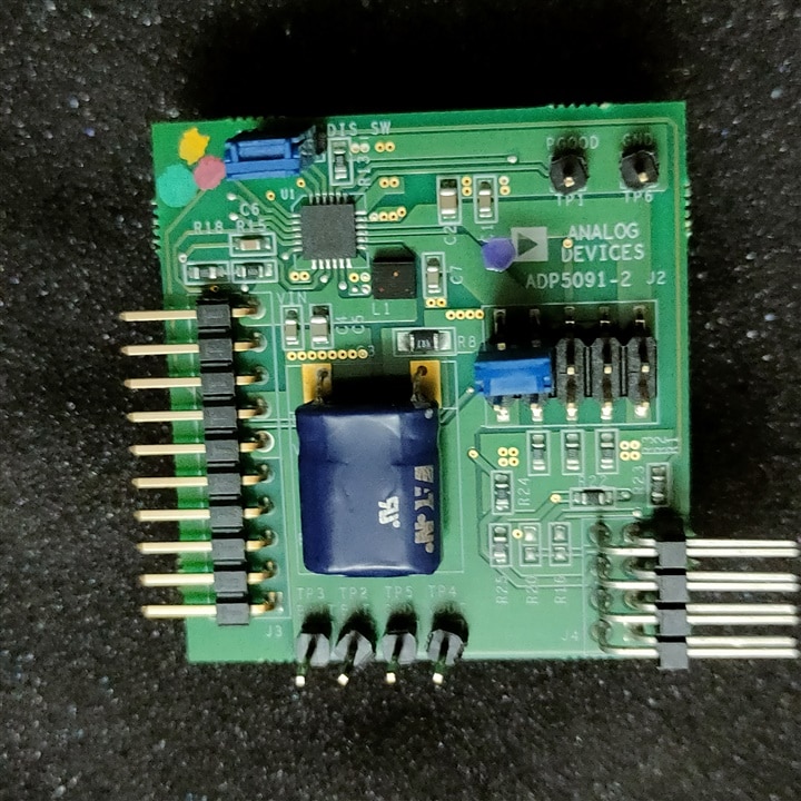
b) Back of Analog ADP5091-2 Evaluation Board

4) ADP509x PV Board
(a) Front of ADP509x PV Board
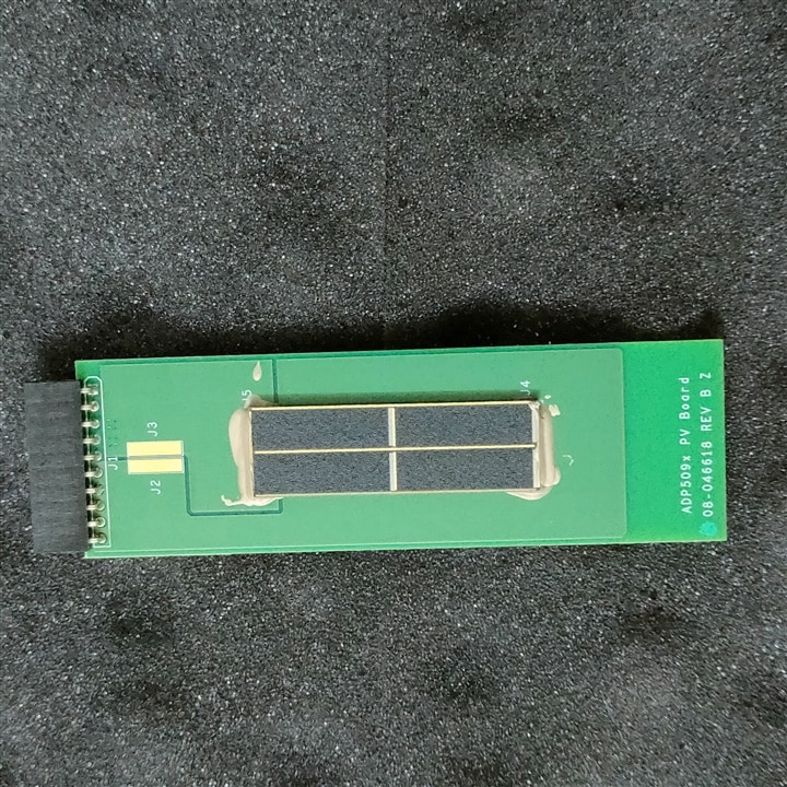
The given solar panel is different than shown on main page of road test.
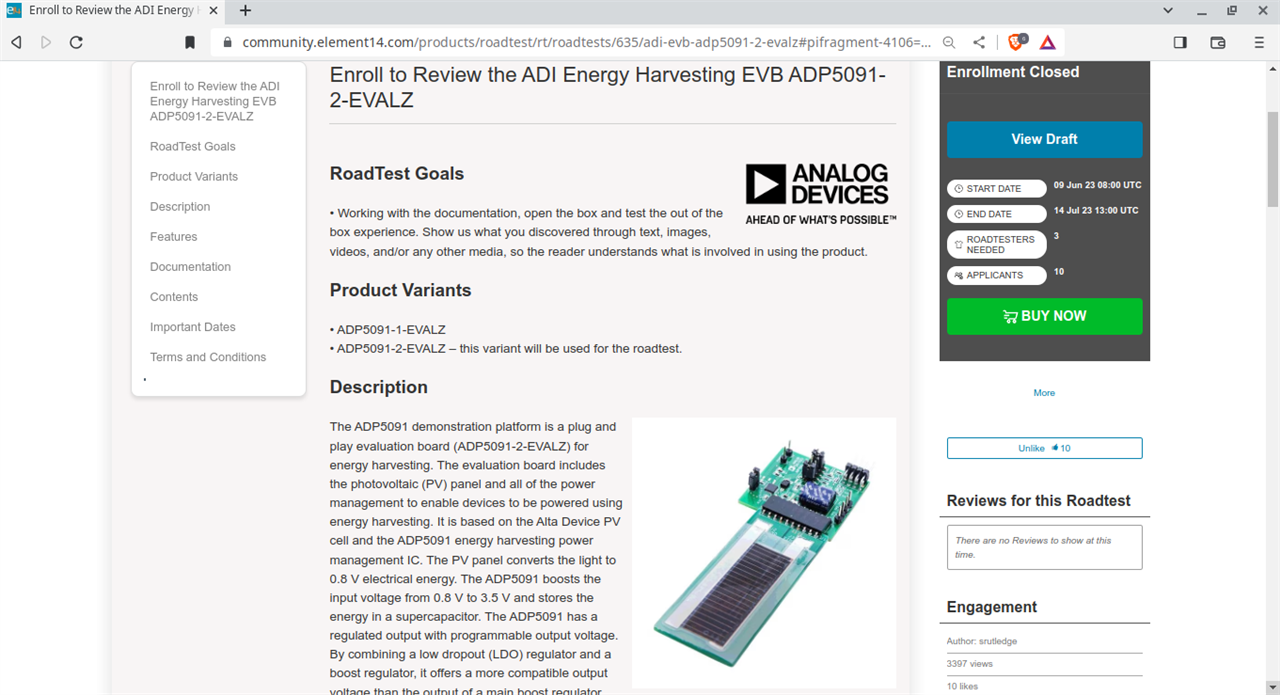
Screenshot as proof
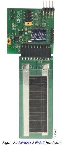
It looks this panel they use to give with other board ADP5090-2-EVALZ
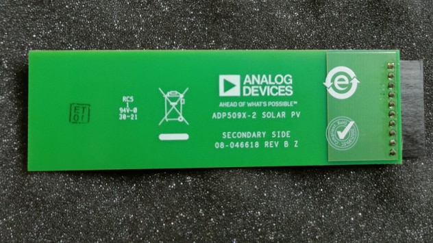
b) Back of ADP509x PV Board
So, what comes from Analog Devices - 'The ADI Energy Harvesting EVB ADP5091-2-EVALZ '
As shown in this unboxing, there are two boards -
On the manufacturer page , there are three main pdfs available from Analog Devices -
Confusion
ADP5091 or ADP5092 or ADP5091-5092 or ADP5091-2-EVALZ
Same thing or All Different ?
Well, ADP5091 is a IC, an integrated circuit on PCB and so this ADP5091 is a energy harvesting power management IC, which is mounted on PCB which has even (supercapacitor for storage).
ADP5092 is another energy harvesting power management IC. So, ADP5091 and ADP5092 are ICs (integrated circuits).
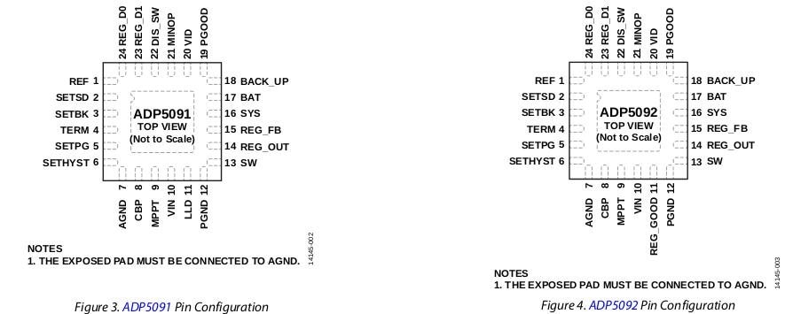
Difference in ICs
And the complete setup, which makes these ICs to work and soldered on PCBs is called an evaluation board.
Now, there are two variants of evaluation board from Analog Devices
2.1 Block Diagram
The system block diagram is

Source : ADP5091-5092.pdf
The above block diagram says - The energy harvesting power management IC, ADP5091 in the ADP5091-2-EVALZ boosts the input voltage from solar panel and the boosted voltage can be taken out using the output connector with different programmable output voltages. This boosted voltage can be storage in energy storage super-capacitor and back-up battery.
2.2 Tables, Functional & Circuit Operation Diagrams
Following are tables, functional diagrams and other important circuit operation diagrams which explains how energy harvesting power management IC, ADP5091 works (Source : ADP5091-5092.pdf). As this is evaluation of boards, I won't go into explaining any of the following diagrams or tables but I will explain all other things, which would be needed by ordinary buyer & evaluation related to it.
| {gallery}Functional Diagrams |
|---|
|
Typical Application Circuit |
|
Detailed Functional Block Diagram |
|
Fast Cold Start-Up Sequence |
|
Program Paramater Setting |
|
Power Switches Structure |
|
Various Threshold Voltages States |
|
Power Path Working State |
|
Programming Threshold Resistors |
|
Outline Dimensions |
2.3 Programmable Output Voltages
As mentioned above, ADP5091-2-EVALZ gives different programmable output voltages, below is the table for 8 different output voltages which are generated from LDO regulator
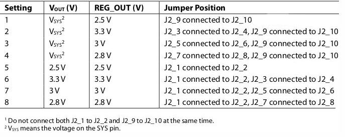
Caution : When doing any of the above mentioned 8 jumper settings, Do not connect both J2_1 to J2_2 and J2_9 to J2_10 at the same time.
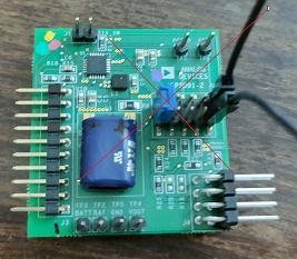
Do not connect the blue jumper and the jumper at black connector (in this pic shown separate) at the same time as per caution.
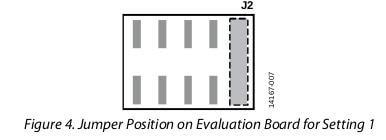
2.3.1 Setting 1 : 2.5 VDC
In this setting, jumper positions J2_9 connected to J2_10.
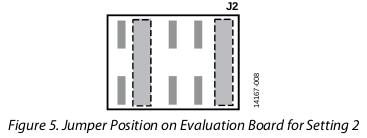
2.3.2 Setting 2 : 3.3 VDC
In this setting, jumper positions J2_3 connected to J2_4, J2_9 connected to J2_10
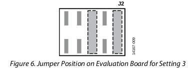
2.3.3 Setting 3 : 3.0 VDC
In this setting, jumper positions J2_5 connected to J2_6, J2_9 connected to J2_10
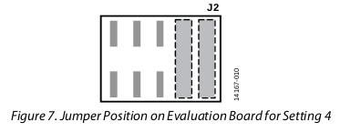
2.3.4 Setting 4 : 2.8 VDC
In this setting, jumper positions J2_7 connected to J2_8, J2_9 connected to J2_10
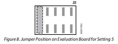
2.3.5 Setting 5 : 2.5 VDC
In this setting, jumper positions J2_1 connected to J2_2
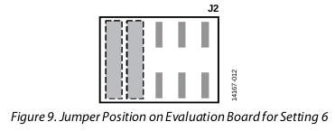
2.3.6 Setting 6 : 3.3 VDC
In this setting, jumper positions J2_1 connected to J2_2, J2_3 connected to J2_4
2.3.7 Setting 7 : 3.0 VDC
In this setting, jumper positions J2_1 connected to J2_2, J2_5 connected to J2_6
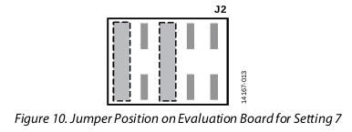
2.3.8 Setting 8 : 2.8 VDC
In this setting, jumper positions J2_1 connected to J2_2, J2_7 connected to J2_8
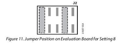
2.4 Caution : Absolute Maximum Input
As mentioned in the unboxing section, the PV board (given for evaluation) can be replaced with some other PV board (next section mentions recommended PV) but it need not only PV Board, it can be Thermoelectric Generator or Piezoelectric Generator or even AC-DC, thus can be used in different applications like photovoltaic (PV) cell energy harvesting or thermoelectric generators (TEGs) energy harvesting or industrial monitoring or self powered wireless sensor devices or portable and wearable devices etc.
But in any of the inputs, the maximum output of say like in our case, Alta Devices PV Panel must not exceed +3.6 VDC. In the next section, I m showing panel voltage varies from 0.2 to 2.36 but it must not exceed + 3.6 VDC.
The absolute maximum rating is - 0.3 V to + 3.6 V. Thus, this input must not also fall below -0.3 V DC.
Confusion : What will happen if it will fall below 0.3 V or above 3.6V, will it damage component
Cheatsheet : There will be no component damage if below 0.3 V. ADP5091-2-EVALZ board needs minimum 0.3 V to work but above +3.6, it will damage it.
The absolute maximum rating for DIS_SW, TERM, SETPG, SETSD, SETBK, PGOOD, SETHYST, REF, REG_D0, VID,REG_D1, LLD, REG_GOOD to AGNDSW, SYS, BAT, BACK_UP, REG_OUT,REG_FB to PGND is - 0.3 V to + 6 V.
2.5 Selecting Energy harvester
This ADP5091-2-EVALZ board operates like out of air as no AC input or no AC-DC input or no battery source. But it do has input source which is mentioned in sub-section 2.4, it can be Solar/PV geneartor or Thermoelectric Generator or Piezoelectric Generator or even AC-DC, and the energy harvesting device has to obey absolute maximum rating.
The selection of input is not limited to the provided Alta Devices PV board but it can be any source which provide minimum of 0.3 V or 380 mV or 0.38V.
The four inputs are mentioned in section 2.8 (Practical Application Schematics).
2.6 Selecting Energy Storage Element
The ADP5091-2-EVALZ support many types of storage elements, such as rechargeable batteries, super capacitors, and conventional capacitors.
2.7 Super-capacitor
The default onboard storage element given is Super-capacitor, labelled as C3 from vendor Cooper Bussmann. The part number is PB-5R0H104-R, has Electrochemical Double Layer Capacitor (EDLC) construction, working voltage of 5 VDC, surge voltage of 6 VDC, capacitance tolerance of -20% to +80% (+20° Celsius), operating temperature range of -25°Celsius to +70°Celsius (extended to +85°Celsius) and capacitance of 0.1 F(Farads).
At 100 Hz, the max. ESR(Equivalent Series Resistance) is 4.0 Ω.
After 72 hrs of operation, nominal leakage current at +20° Celsius is 3 μA (micro-amperes).
The lifetime performance is 1000 hours with capacitance change ≤ 30% of initial value and ESR change is ≤ 300% of max. initial value. This is calculated at two voltages at two operating temperatures -
2.8 Practical Application Schematics
There are four circuit schematics with component values given in the datasheet. I have used the circuit 1 and circuit 4 for evaluation of ADP5091-2-EVALZ board. The for four different input sources are
| {gallery} Practical Application Schematics |
|---|
|
Input Source : Alta Devices PV Board |
|
Input Source : Thermoelectric Generator |
|
Input Source : Piezoelectric Generator |
|
Input Source : AC |
2.9 Chosen Circuits For Evaluating ADP5091-2-EVALZ
In the Section 5 'Practical Evaluation of ADP5091-2-EVALZ Board', on the following chosen circuits, ADP5091-2-EVALZ is practically evaluated.
1) The 'Alta Devices PV Board' is provided with this kit.
2) Input AC is 230 VAC which is step down to 0.3V - 3.3 V. This step down can be achieved in many ways. I have used AES-ULTRA96-V2-G and Click Mezzanine to achieve 0.3V - 3.3 V.
AES-ULTRA96-V2-G needs 12V supply from 230VAC (96Boards 4A Supply (AES-ACC-U96-4APWR ) 12V, 4A) but board has 40-pin header which has 2 pins which generates 1.8V and 5V.
Click Mezzanine (96Boards Click Mezzanine Starter Kit, AES-ACC-U96-ME-SK ) generates 3.3V.
2.10 Board Connections in Simple Language & My Test Plan
The ADP5091-2-EVALZ has 2 connectors (J3 & J4) , 2 places where jumpers ( J1 & J2) can be placed and 2 places are six test points- ( TP1, TP2, TP3, TP4, TP5, T6).
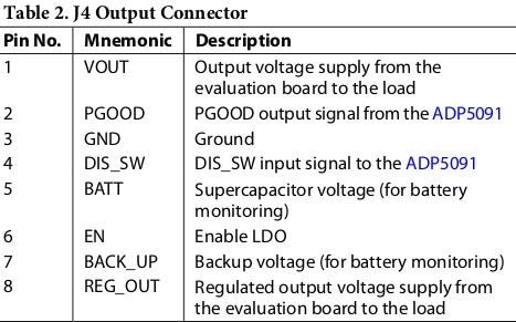
So, My plan is to connect 3 multimeters at the three Test Points (TP2, TP3, TP4) and one multimeter at the input source point at J3, and try all jumper settings with enable and disable boost and try to lit LED, DC motor from the output.
3. Evaluation of Alta Devices PV/Solar Board
The datasheet recommends four PV devices

But, a solar panel given with this ADP5091-2-EVALZ is of Alta Devices.
Rating of this panel given in datasheet is 0.72 V, 42 μA
and PV board consists of four solar cells. So, the max. voltage should reach 0.72 x 4 = 2.88 VDC or 2.88 Voc (open-circuit voltage).
The indoor environments has typical lux levels of 200 lux to 1000 lux, which gives around 0.38 VDC from this Alta Devices PV board, which is << 2.88 VDC. The ADP5091 IC boosts this 0.38 VDC to 3.3 VDC.
Alta Devices Solar Panel Construction
This solar cell is made of a semiconductor, Gallium Arsenide (GaAs) interconnected in cubic lattices. This solar technology on GaAs being an expensive material, has the highest efficiency currently available in the world and is used only for satellites, spacecraft, RF or military applications.
Alta Devices produces this cell as a very thin layer of GaAs  using Metal organic chemical vapor deposition (MOCVD or MOVPE) reaction of trimethylgallium
  and arsine
  in a proprietary process. Alta Devices solar cell is made by growing a thin film (1-2 microns thick) of GaAs on top of a high purity GaAs wafer, which is then separated from the wafer for usage as a solar cell while the wafer is reused.
This solar board has 10-pin connector instead of 2 pin. I have found in hard way, which pin is +, -, testing with each pin but later I found it is given in datasheet (ADP5091-2-EVALZ-UG-927.pdf, page 6), this should be mentioned separately.

Source : ADP5091-2-EVALZ-UG-927.pdf, page 6
Note : Pins are 10 and 7 but I had earlier labelled as pin 10 as pin1 and pin 7 as pin4, so in all my video recordings, this error would be there. Though this error wont be in this typed review.

Note : The pins labelled in black are pins 10 (not pin 1) and pin 7 (not pin 4) .
The solar cell paste/glue is turned muddy or the paste is de-colored but not deteriorated as the glue is still firmly holding panel.
This glue is also conductive, that is instead at the pins, the same voltage can be measured keeping the probe on this paste only.
I have measured voltage w.r.t to - (pin 7) on all pins and only at pin 10 which is +, it shows some voltage reading, and on rest other 8 pins, reading is 0.
I measured in different room temperatures, ambient temp. and sunlight. Following are videos from PV board only ( Note : the evaluation module is not connected)
3.1 ) Video 1 - PV Board
Video demonstrates the increase of voltage, if a tubelight is turned on and/or if a second camera mobile torch is turned on.
The minus sign is wrong polarity, the max. voltage is 1.26 VDC (can be seen at 1:00 of the recording) with indoor conditions at 7:24pm IST.
You don't have permission to edit metadata of this video.
3.2 ) Video 2 - PV Board
Video is taken in afternoon around 1:20 pm IST, open atmosphere, and the max. voltage is 2.30 VDC
You don't have permission to edit metadata of this video.
3.3 ) Video 3 - PV Board
The maximum output voltage from Alta Device PV Board is 2.36 VDC, with temperature conditions of Delhi,India dated 7 Sept 2023 at 2:14pm IST . At this time of recording, it was very hot in between with cloudy conditions. This max. voltage of 2.36 VDC can be seen between 2:04 - 2:09 of the recording.
You don't have permission to edit metadata of this video.
3.4 ) Video 4 - PV Board
Max. Voltage reached in Sunlight = 2.49 VDC, at 0:06 of the recording.
You don't have permission to edit metadata of this video.
3.5) Video 5 - PV Board
Max. Voltage reached in Sunlight = 2.49 VDC at 0:50 of the recording.
2.46 VDC can be seen at 0:30 and 0:34 of the recording.
You don't have permission to edit metadata of this video.
3.6) Video 6 - PV Board
Under sunlight with shade, the PV panel was fluctuating from 1.84 V - 1.95 V. At 0:05, incandescent bulb 25W in switched off position is placed over PV panel board, and the reading was still around 1.84 VDC.
At 0:15 of the recording, the bulb is turned on and the voltage is 2.48V
At 0:24 of the recording, the bulb is turned away from the panel and the voltage falls to 2.17 V
At 0:27 of the recording, the max. voltage reached is 2.50 VDC.
You don't have permission to edit metadata of this video.
3.7) Video 7 - PV Board
You don't have permission to edit metadata of this video.
3.8) Video 8 - PV Board
You don't have permission to edit metadata of this video.
3.9) Video 9 - PV Board
Alta Devices PV board Conclusion
I have done separate and standalone reviewing and analysis for 'Alta Devices PV board' besides reviewing ADP5091-2-EVALZ. This 'Alta Devices PV board' can be replaced with any other source(mentioned) or other vendor. The videos has shown that this 'Alta Devices PV board' is light sensitive, it responds to any light source whether natural/supernatural Sun or ambient or artificial. 'Alta Devices PV board' has responded to voltage increase from LED, incandescent bulb, mobile torch. The output voltages are satisfactory as per datasheet claim, reached 2.58 VDC with VOC (max) of 2.88 VDC.
4. Plots/Performance Characteristics of ADP5091-2-EVALZ
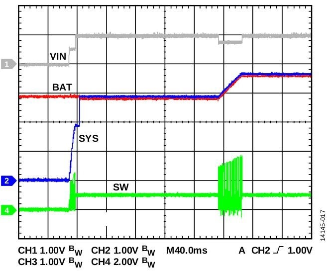
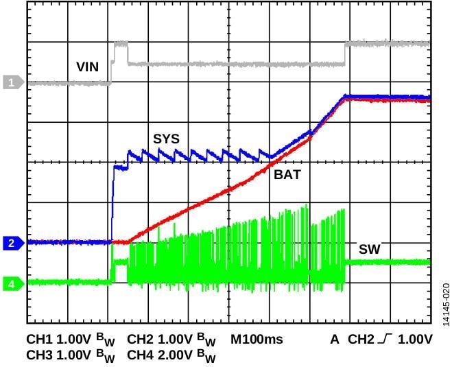
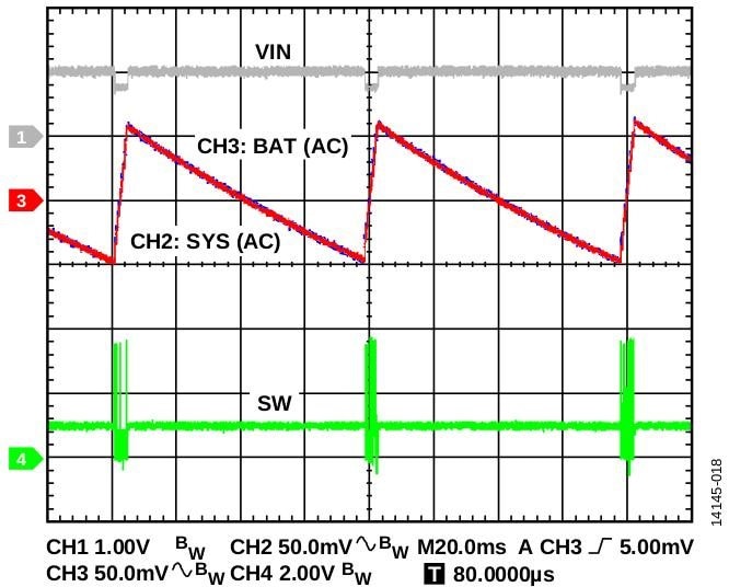
Analog Devices has provided following 36 graphs in 25 categories in its datasheet. (Note : These are not measured or plotted by mine oscilloscope but by Analog Devices. Source : ADP5091-5092.pdf)
4.1 Efficiency vs. Input Voltage
| {gallery}Efficiency vs. Input Voltage |
|---|
|
Input Current : 10 μA |
|
Input Current : 100 μA |
|
Input Current : 10 mA |
|
Input Voltage : 0.5 VDC |
|
Input Voltage : 1 VDC |
|
Input Voltage : 2 VDC |
4.2 Efficiency vs. Input Current
| {gallery} Efficiency vs. Input Current |
|---|
|
Input Voltage : 0.2 VDC |
|
VIN = 0.5 V, VREG_OUT = 2 V, IREG_OUT = 10 μA |
|
VIN = 1 V, VREG_OUT = 2 V, IREG_OUT = 10 μA |
4.3 Quiescent Current vs. SYS Voltage
| {gallery}Quiescent Current vs. SYS Voltage |
|---|
|
VMINOP ≤ VCBP |
|
VREG_D0 = VREG_D1 = VSYS, VMINOP ≤ VCBP |
|
VMINOP > VCBP |
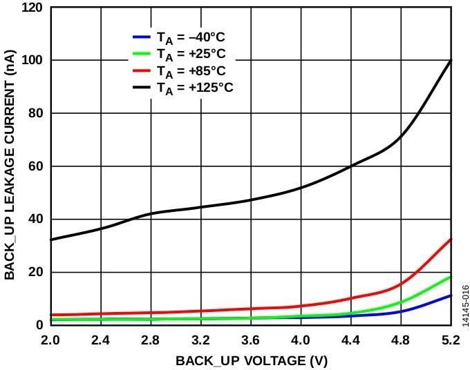
4.4 BACK_UP Leakage Current vs. BACK_UP Voltage
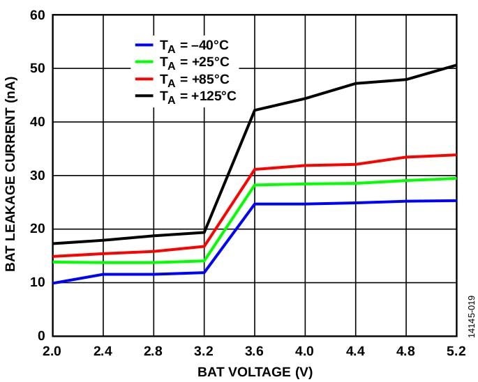
4.5 BAT Leakage Current vs. BAT Voltage
4.6 Startup with Battery
4.7 Startup with Capacitor
4.8 Output Ripple
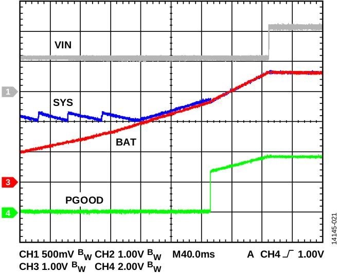
4.9 PGOOD Function
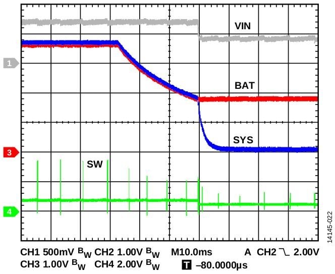
4.10 Battery Protection Function
4.11 BACK_UP Function
| {gallery}BACK_UP Function |
|---|
|
VBAT < VSETBK, VBACK_UP < VBAT |
|
VBAT < VSETBK, VBACK_UP > VBAT |
|
VBAT > VSETBK, VBACK_UP > VBAT |
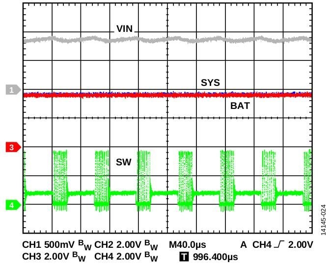
4.12 Boost Pulse Frequency Modulation (PFM)
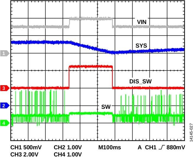
4.13 DIS_SW Function
4.14 MPPT (Maximum Power Point Tracking) No Sensing Mode
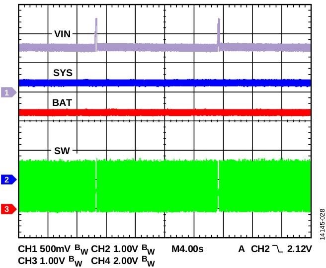
4.15 MPPT (Maximum Power Point Tracking) Dynamic Sensing Mode
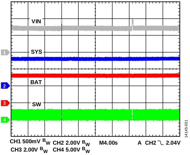
4.16 MINOP (Minimum Operation threshold) Function
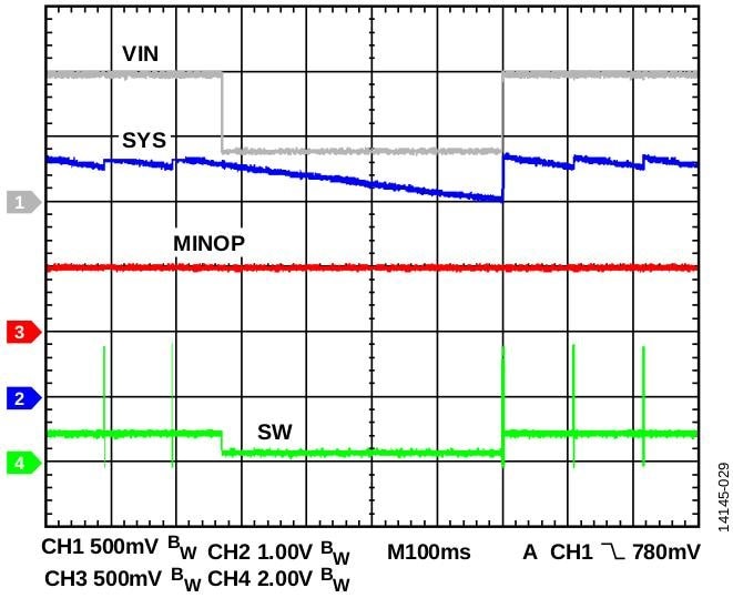
4.17 LLD (Low Light Density) Function
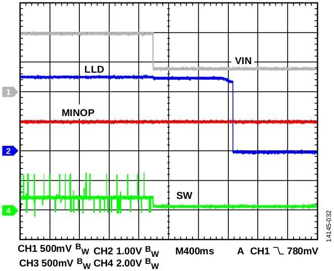
4.18 Hybrid Mode
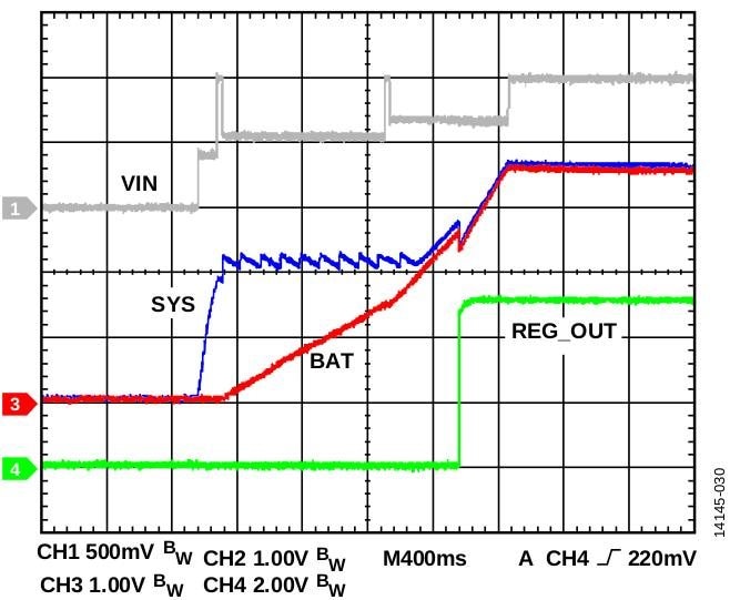
4.19 Boost Mode
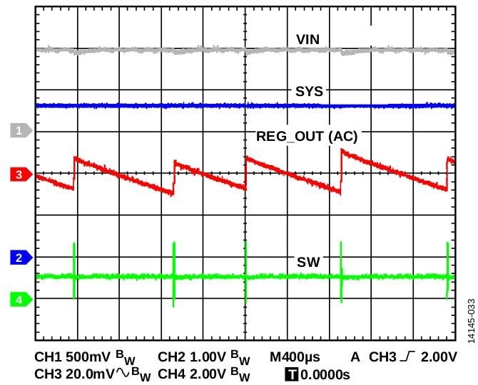
4.20 REG_GOOD Function
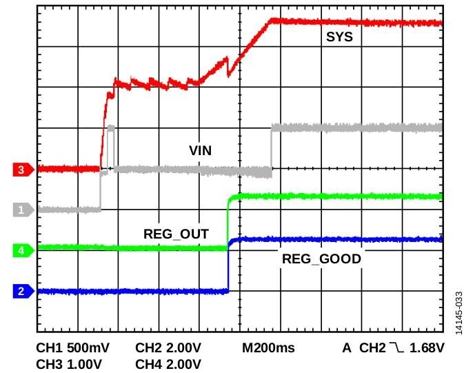
4.21 REG_OUT Load Transient, Hybrid
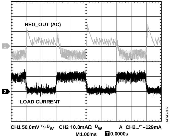
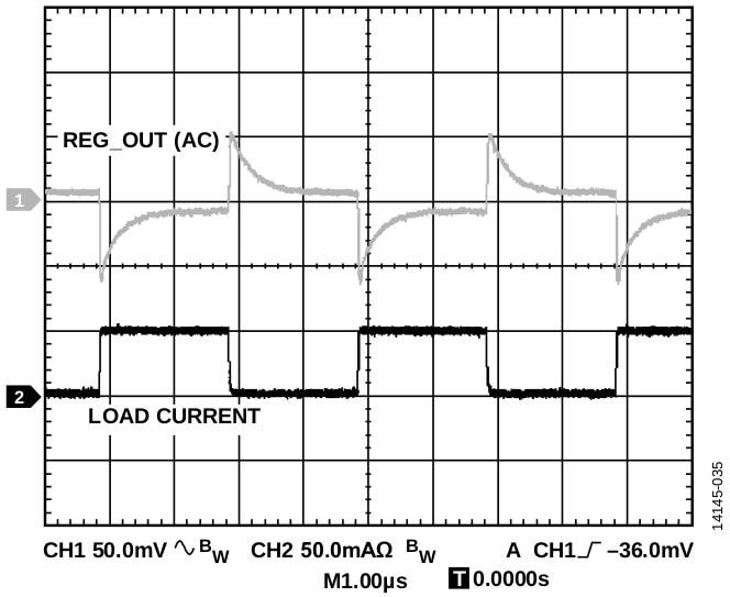
4.22 REG_OUT Load Transient, LDO
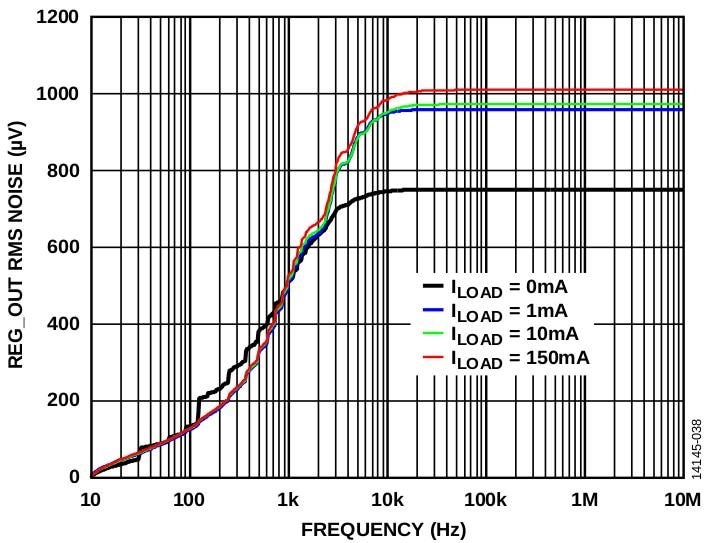
4.23 REG_OUT RMS Noise vs. Frequency
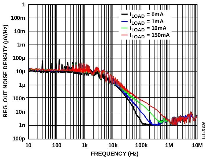
4.24 REG_OUT Noise Density vs. Frequency
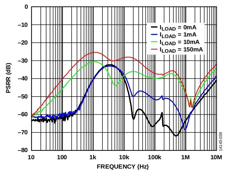
4.25 Power Supply Rejection Ratio (PSRR) vs. Frequency
5. Practical Evaluation of ADP5091-2-EVALZ Board
As mentioned in Section 2.10, my plan is to connect 3 multimeters at the three Test Points (TP2, TP3, TP4) and one multimeter at the input source point at J3, and try all jumper settings with enable and disable boost and try to lit LED, DC motor from the output.
The three multimeters at TP2, TP3 & TP4 have white stickers labelled as VOUT, BAT, BATT
1) Testing Video 1
2) Testing Video 2
3) Testing Video 3
You don't have permission to edit metadata of this video.
4) Testing Video 4
You don't have permission to edit metadata of this video.
5) Testing Video 5
You don't have permission to edit metadata of this video.
6) Testing Video 6
You don't have permission to edit metadata of this video.
7) Testing Video 7
You don't have permission to edit metadata of this video.
8) Testing Video 8
You don't have permission to edit metadata of this video.
9) Testing Video 9
You don't have permission to edit metadata of this video.
10) Testing Video 10
You don't have permission to edit metadata of this video.
11) Testing Video 11
You don't have permission to edit metadata of this video.
12) Testing Video 12
You don't have permission to edit metadata of this video.
13) Testing Video 13
You don't have permission to edit metadata of this video.
14) Testing Video 14
You don't have permission to edit metadata of this video.
15) Testing Video 15
You don't have permission to edit metadata of this video.
16) Testing Video 16
You don't have permission to edit metadata of this video.
17) Testing Video 17
You don't have permission to edit metadata of this video.
18) Testing Video 18
You don't have permission to edit metadata of this video.
19) Testing Video 19
You don't have permission to edit metadata of this video.
20) Testing Video 20
You don't have permission to edit metadata of this video.
21) Testing Video 21
You don't have permission to edit metadata of this video.
22) Testing Video 22
You don't have permission to edit metadata of this video.
23) Testing Video 23
You don't have permission to edit metadata of this video.
6. Some Cons
Following are cons (not mentioned according to priority). For positive points pls see conclusion. The product comes in very good packaging. The evaluation board is CE and CMC qualified, and RoHS (Restriction of Hazardous Substances ) complaint and certified. This product is RoHS Compliant RoHS Phthalates Compliant. There is no SVHC (Substances of Very High Concern). The 6-digit HSN (Harmonized System of Nomenclature) code is 85381090, EU Export Control Classification Number is NLR and the US Export Control Classification Number is EAR99.
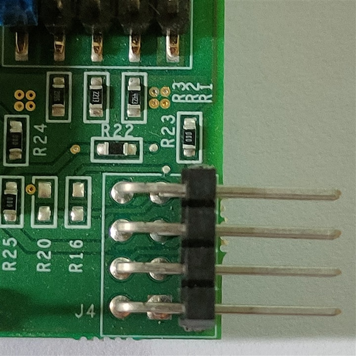
1) The J4 has no marking of pins where to find pin 1 or pin 3 or pin 8
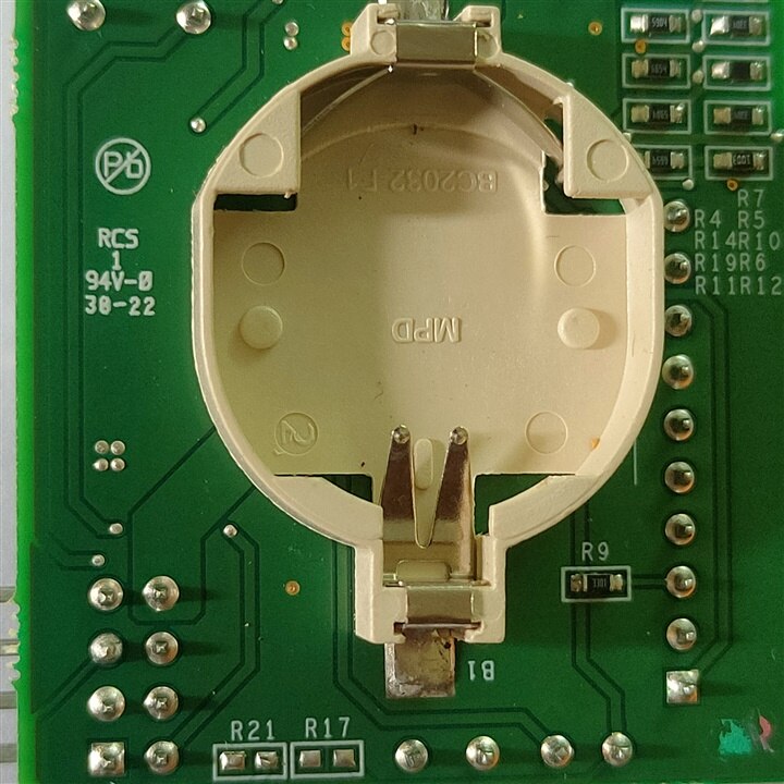
2) In the above picture even battery holder can be seen, plus , minus not marked
3) Of all documentations given, no documentation explains coin battery is what and whether it is a coin battery for what (for newbies). Only ADP5091-5092.pdf mentions on Page No. 25 and 26 and that too under 'Typical Application Circuits' - (a) Panasonic Primary Li-Ion Coin Cell CR2032 as the Backup and Battery [Page 25, Fig. 45] , (b) Panasonic Primary Li-Ion Coin Cell CR2032 as the Backup Battery [Page 25, Fig. 46], (c) Panasonic Primary Li-Ion Coin Cell CR2032 as the Backup Battery [Page 26, Fig. 47]
4) Documentation can be confusing which kind batteries can be used as rechargeable batteries, no where mentioned. The above mentioned CR2032 is very popular and comes as non-rechargeable, which can be mistaken, backup storage energy path, an integrated backup controller, a
Novice can buy wrong battery type which can cause damage to board or may be explosion as super-capacitor is there, which may lead to an electrical shock, fire hazard , personal injury,explosion,property damage or may be death ! So, this back-up battery must be given and properly documented.
I had worked on prototypes where capacitors had physically exploded.
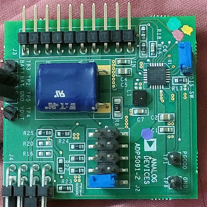
5) Similarly, pins of J2, J3 not labelled. J3 is connected to solar panel, so no struggle in finding pin 1 or pin 10 but PCB should have pins labelled.
6) Poor Quality plastic holder
| {gallery} Poor Quality plastic of holder |
|---|
|
Initially |
|
IMAGE |
|
Broken pieces kept on battery |
7) 2 jumpers are given but 1 more is required. (black jumper I had to arrange)
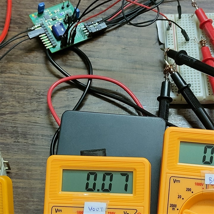
8) Jumper 1, not explained properly
7. Comparable Products
Following prices are without tax and without shipping (and/or custom charges).
The currency conversion from INR to USD is taken from the website. The amount mentioned in Euro,€ is obtained after INR currency conversion to Euros, €.
The evaluation board ADP5091-2-EVALZ has price tag of Indian Rupees INR Rs.4,801.22, British pound sterling GBP of £48.46 , Chinese Yuan CNY 472.7355, Euros € 53.40 and US Dollars $ 57.67 There are four competitive and comparable products, whose pricing and pros cons are mentioned below :
1. MAX20361EVKIT#
This evaluation kit is from Analog Devices only but the input source intended is solar only and is Single/Multi-Cell Solar Harvester from manufacturer. This comes with demo software as compared to this product 'ADP5091-2-EVALZ '. MAX20361EVKIT# kit requires USB2PMB2 adapter board, USB A to micro-B cable, Windows PC with USB ports & DC power supply. All these are eliminated in ADP5091-2-EVALZ .
Th MAX20361EVKIT# kit has price tag of Indian Rupees INR Rs 5,857.23, British pound sterling GBP of £51.56 and US Dollars $67.58 .
The price is also higher, so ADP5091-2-EVALZ is winner.
2. STEVAL-ISV020V1
The STEVAL-ISV020V1 is from ST Microelectronics and is also an energy harvester and battery charger. The datasheet says any battery chemistry- lithium, NiMH, solid state thin film or supercapacitor can be charged. But it has limitation, STEVAL-ISV020V1 board is optimised to harvest energy from PV panels supplying 2.6V ≤ V(pv panel) ≤ 9V.
The STEVAL-ISV020V1 has price tag of Indian Rupees INR Rs 3,441.23 , British pound sterling GBP of £33.27 and US Dollars $ 40.80.
ADP5091-2-EVALZ works with 380mV (cold start) or 0.3V rather than 2.6 V, as ADP5091-2-EVALZ has charge pump.
3. STEVAL-ISV019V1
The STEVAL-ISV019V1 is from ST Microelectronics and is also an energy harvester and battery charger. The datasheet says any battery chemistry- lithium, NiMH, solid state thin film or supercapacitor can be charged. But it has limitation, STEVAL-ISV019V1 board is optimized to harvest energy from PV panels supplying 0.5V ≤ V(pv panel) ≤ 2.5V.
The STEVAL-ISV019V1 has price tag of Indian Rupees INR Rs 3,460.49 , British pound sterling GBP of £34.31 and US Dollars $42.08.
ADP5091-2-EVALZ works with 0.3V, which is > 0.5 V of STEVAL-ISV019V1
4. EM8500
EM8500 is an IC not an evaluation board but it takes same minimum voltage level of 0.3 V like ADP5091-2-EVALZ and allows same inputs like solar panel or Thermo-electrical generator (TEG).
EM8500 is very close competitor to IC, ADP5091.
There are few other products but they are not universal like ADP5091-2-EVALZ as some can take only Piezo input, there are few ICs like EM8500 which are very near competitive. The other comparable competitive products are from Analog Devices only and it's variants - ADP5090-2-EVALZ and ADP5091-1-EVALZ.
8. Conclusion
I have gone into the detailed explanation of datasheet, not sure if it would be liked or not but for me it is complete product reviewing and I have still missed out theory of operation and the explanation of functional block diagram (which is irrelevant for product viewing). The various settings, connections possible with micro-controller, performance characteristics are product features and need to be explained besides practical evaluation of board.
The documentation is quiet complete (& generally documentations are of these many pages only, 28 + 9 pages) due to various settings and functionalities. There is no Demo Software applicable for this product, so I am taking Demo Software equivalent to documentation and rated as 5/5.
The product comes with excellent packaging with soft pads to protect components damage and the deserving separate photo-shot is given.
I have done reviewing not for 1 product but 2 separate products - ADP5091-2-EVALZ and Alta Devices PV Board.
In the review of 'Alta Devices PV Board', I have measured in different room temperatures, ambient temperature, sunlight and different light sources. I used ordinary tubelight, led tubelight, mobile torch, 9W LED bulb, incandescent bulbs of 25 W, 40W, 100W.
I had turned on two 100 W bulbs but the turning of the second bulb produced voltage difference of 0.01- 0.03 VDC.
The use of 9W LED bulb resulted in lesser increase of voltage than 25W/40W incandescent bulb. And when with a 9W LED bulb, a 100 W incandescent bulb is lit, the voltage increased by approx 1 volt - 1.20 VDC.
The overall result was very satisfactory and the max. voltage has reached to 2.58 VDC in the ambient light without any external source (unfortunately when I measured this , camera was off) but it didn't reached to 2.88 VDC at-least in this review; it may rise to 2.88 in open field.
As the input can be other than Alta Devices PV board, I have taken other input as AC source of 230 VAC, which is stepped down to acceptable level of 3.3 V. For this I have used AVNET Ultra96 V2-G and 96Boards Click Mezzanine Starter Kit.
The booster circuit didn't worked as my expectations! Still, Analog Devices must revise PCB as it is competitive market product & it may be used for WSN, HVAC, building and home automation, industrial control, access control, smart lighting, asset and livestock positioning and tracking, surveillance or Analog Devices may improve booster circuit!
I have tried output to drive 5V DC motor but voltage is lower than needed by a 5V DC motor but 2 different LEDs are able to lighten up.
In the future work, I may interface with micro-controller as my two micro-controllers dead(& thrown) and also with FPGA (AES-ULTRA96-V2-G) and may use in my personal R&D.
