RoadTest: Infineon Gate Driver with Truly Differential Input
Author: Jan Cumps
Creation date:
Evaluation Type: Power Supplies
Did you receive all parts the manufacturer stated would be included in the package?: True
What other parts do you consider comparable to this product?: traditional gate drivers for both High side and Low side
What were the biggest problems encountered?: evaluation board manufacturing quality (solder bridge)
Detailed Review:
The Infineon differential input gate driver is one of those components that you get to know by accident. One of those where you are glad that you learned about it, because it solves a real problem in an easy manner.
Ground noise in heavy duty designs is a thing. High current can lift the ground level of (part of your) circuit. Heavy duty loads can induce ac noise on the ground too. This driver is designed towork under those conditions. |
Infineon uses differential inputs as an interesting approach to solve several FET gate drive hurdles.
There are two inputs per driver, and the driver is driven by the difference between those signals.
This is different to the more common single input gate driver solution, where the driver's input signal is referenced relative to the driver's ground potential.
For low side FETs in a half bridge, where the sink is usually close to the circuit ground level, AC noise and DC ground lift may impact the input level the gate driver sees.
With the differential approach of the 1EDN8550B, whatever happens with the source pin voltage has limited impact on the logic inputs of the gate driver.
The evaluation board lets you play with drift between the controller signal ground and the low side driver's source pin - so you can create these events in a lab and measure the circuit's stability.
The effect is more spectacular on the high side, where the driver can be driven by the microcontroller's 3.3 V signals while the (effective) ground level of that driver is at 48 V.
That 48 V PWM signal is in essense superimposed on the ground of that upper side driver ground - way wilder than what you can modulate on the low side.
This part of the circuit arguably shows the strength of the differential inputs most.
I'm trying to show that in the image below, where the relative ground point of the high side (the point where the driver IC ground and the power FET sink connect),
wildly jumps between 0 and 48 V - including some switching noise and overshoot.
Still, the high side driver happily works with the 3.3 V inputs, even when the ground level of those two inputs is at times 48 V below the driver ICs ground level.

image source: heavily edited figure 2 of Infineon's evaluation board Application note
This is because the driver isn't controlled by the level betwen the control signals and (some) ground, but by the difference between the two inverse inputs.
Below you can see that differential signal.
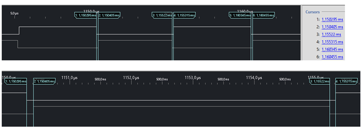
image: capture of the PWM_HS and PWM_LS signals with a logic analyser
Both high and low side drivers are controlled by the same signal, but inverse.
Where the HS goes to the IN+ on the high side driver, it's connected to the IN- on the low side driver.
And vice versa for the LS PWM signal.
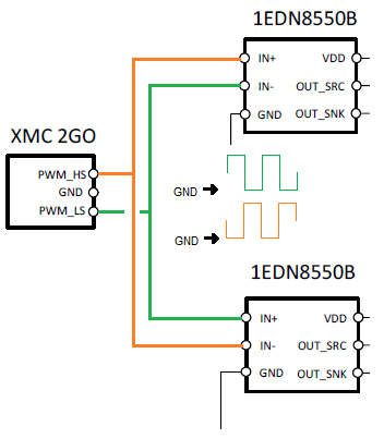
image source: again an edit based on figure 2 of Infineon's evaluation board Application note
There are four parts to this. A few very prominent, and the best part a little bit downplayed.
You can put the low side driver to the test by messing with it's ground level - literally pulling away the base under it's feet. Like what happens in real life high power circuits.
Under both conditions, it performs as if not a lot is going on.
It can keep on driving the FET, because the FET's sink drifts away at the same level as the driver's ground.
And it keeps on accepting the input signal (whatever that signal ground level is related to the driver's ground).
Because the input signal that controls the driver is differential. The IC is driven by the difference between the high and low.
The ground level of these signal plays no role in the equation, so drift does not matter (within specs of course).

You see the difference when you simulate the identical offset or AC noise to a non-differential driver.
Because that signal is referenced to the IC's ground, drift directly influences the input to the gate driver. And significant noise and drift can make the driver open o close when it shouldn't.
I will show the behaviour of the circuit with a non-differential driver in a separate blog.
Yes. There's more to learn on the board than the core business.
This,is a nice circuit that's used in many half-bridge designs.

image source: again an edit based on figure 2 of Infineon's evaluation board Application note
It's easy to power the low side controller of a half bridge. Because it bum sticks to the ground. You just need to supply the IC with the correct voltage (in our case: 12 V).
The high side is different though. It's ground level (it is the green part above: the switch node) heavily jumps between 0 and 48 V. What do we have to supply as power to the IC? 12 V? 60 V? Does the supply have to bump with the relative ground, at 100 kHz?
The bootstrap circuit helps. It's a diode and a capacitor.
When the half bridge is driven low, power is supplied via the 12 V supply (that also takes care of the low side driver).
In the mean time, the bootstrap capacitor is charged by that same 12 V supply via the bootstrap diode.
When the switching node jumps high (to 48 V). The capacitor's low side jumps high along. And it's upside is charged to 12 V, so it's at 60 V level.
For the high side IC, this shows as a voltage of (60 V - 48 V) 12 V. Exactly what the IC needs.
What a great circuit.
To mimic the ground lift or sink cause by a heavy load, this board uses a little simulation circuit.

image source: why draw a circuit with the control on the right and the output on the left?
The circuit - a quad opamp that (in this configuration with 4 in parallel can drive and sink the current used by the gate drivers vs the offset generated XMC 2 GO) allows to lift and sink the ground by almost +- 12 V.
rant: I am absolutely no fan of how this circuit schematic is drawn. The four opamps provide exactly the same function but it looks like it's three the same and one special.
And right-to-left control flow?
It would be more intuitive if this simple circuit was drawn as the simple circuit it is. Why confuse the reader by ignoring settled circuit conventions?
Infineon made great use of PCB trace's inherit inductance.

The engineer can change the inductance by soldering away the 0 Ohm resistors (named Jx because J stands for jumper) that shortcut the meanders.
With all resistors in place, the inductance is lowest (straight path).
Step by step you can increase the inductance - and the ac noise - by removing the resistors. The application guide helps you.
A good hand is needed, because they are 0805. But it's doable.
You get a versatile small microcontroller in the package. From Infineon themselves. A nice small dev board with an ARM XMC1100 mcu.
This thing by itself is worth evaluating. Great that Infineon uses its own product here.

For good and bad. They are an excellent way to probe this circuit without the risk of slippage and other bad things that can happen to a probe on a live circuit.
They are also good for signal integrity. These buses may provide one of the best ways to keep the ground loop tight, thus avoiding noise pickup.
They do require matching probes though. That's not a bad thing but it can be an additional cost. There aren't universal solutions that match the majority of probes out there.
This is the first board I saw with these connectors. Most boards either provide test points or ground + test point pairs sized for use with a pigtail ground spring.
It's a TRACO POWER module. Very good and worth incorporating in your product.

(free marketing tip) However, Infineon, as a manufacturer of switch mode components, could have used this part of the board to show off some more of their own product range.
They have the attention of the engineer evaluating that part of their business (the engineer sits with the nose on the board) and could have symbiotically added some hidden product placement. They did it with the microcontroller.
Great. The way Infineon manages to simulate distortion from high power devices with tiny circuits is a revelation.
How you can use an opamp or PCB traces to mimic what happens with ground potential in a circuit with rogue motor, coil driven actuators, high loads...
As indicated in the documentation, power the microcontroller from an external supply (e.g. phone charger). The circuit isn't isolated and you should not power the microcontroller from your PC or laptop.
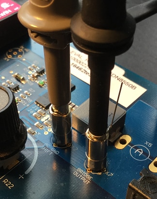
You need to connect the two sides of X5. If you have a current probe, use a bridge that allows you to clamp that probe around it.

The firmware that you can download from Infineon's website can briefly pull both PWM lines high at the start of the code. Half bridges don't like that, so plug in the USB supply, then the 48 V barrel for the whole board.
On the scope capture below you can see the high and low side PWM signal. The orange channel in the middle is the sum of both signals.
Because the signals are differential with dead band, the math channel should never reach 6.6 V. But it does at the few lines of code where the PWM is configured.
If you switch on the microcontroller first, before supplying power to the evaluation board, this will not harm the half bridge.
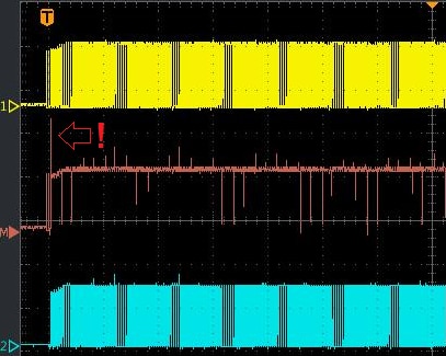
image: the two PWM signals from the XMC 2 Go and a matth signal summing both inputs
The application note (user guide) for this board is extensive and has all the info you need. It's not a good read though.
Somehow it seems it's written without an upfront idea on how to structure it. If you see a graph, it needs digging to find out what it's about.
It should be the other way around, where you know what the graph is about and you dig into it to get a deeper understanding.
The value of this gate driver for the high side of a half bridge is mentioned as the main reason for making this board. But in the document, this is not very well elaborated upon.
I think it's made by the application engineers while designing and trying the circuit.
It can gain from a review by someone who has a little more distance from the subject. They could morph it into a more structured document.
Check the PCB. My kit din't work at first because of a solder bridge that shorted the power of the LS driver.
I'm not a huge fan of vias as footprint for a SOIC pin. Sometimes needed to have an as-short-as-possible connection.
In this design, they could have been avoided because on the other PCB side the trace is wandering of as a long trail (e.g. IC7).
The connection between the switching node and the output inductor is a small via.
For the pass-through of the switching node from top to bottom, four vias are used and I think that's enough for what the adapter can source.
The one via pass-through back from bottom to top at the inductor may be a stretch for the current that the via can transfer.

image source: annotated Figure 21 of Infineon's evaluation board Application note
One of the tests - introducing AC noise on the ground signal with a classic gate driver - is destructive.
The power FETs are exposed to shoot-through and thermal stress out of specs.
Take that into account. Run those at the end, or have spare FETs at hand.
If you change the duty cycle, take care that you don't go (near) 100%. The boostrapping supply on the high side requires that the switch node goes to ground regularly to keep the power of that upper driver going .
The differential gate driver is a good product in designs where noise and drift needs to be addressed. It makes the logic side less dependent on the heavy things going on at he power side.
It's also an option as high side driver - by nature. Because it's resilient to noise on ground, it's also armed against the ground level of a high side driver that switches along with the switch node level.
The board itself and the design is also a good reference and learning point for the engineer.
A great product. A great roadtest opportunity.
| Related Blog |
|---|
| Infineon Gate Driver with Truly Differential Input: Custom Firmware to Control Duty Cycle |


Top Comments
Thanks for the detail in this, especially the PCB design review.
I looked at this roadtest, and decided I'd much rather design the chip into my own device, and there are other reason.
Do we know that…
The parts for further tests arrived. Replacement differential gate drivers 1EDN8550B1EDN8550B, standard low side 1EDN85111EDN8511 gate drivers to test the difference with the differential ones regarding…
Very good road test report.
DAB