RoadTest: Altium CircuitStudio! Roadtest
Author: antosh
Creation date:
Evaluation Type: Independent Products
Did you receive all parts the manufacturer stated would be included in the package?: True
What other parts do you consider comparable to this product?: Experience with Altium Designer, Eagle, Diptrace Also considered KiCad, Target 3001!
What were the biggest problems encountered?: Library management, current documentation of features included
Detailed Review:
So, after weeks of using Altium Circuit Studio (CS), it is time to post a review. To read more about me, talk a look at this blog post and first comment https://www.element14.com/community/people/antosh/blog/2016/09/19/altium-circuit-studio-roadtester. The very brief version is I’ve designed and made PCBs for a long time and have a couple years’ experience with Altium Designer (AD), up to AD14.
Overall I liked CS. The user interface took a little bit of time to get used to, but I was usually pleasantly surprised with the ease to find what I was looking for. I did run into a few user interface aspects that seemed inconsistent and two problems that could cause users errors with their designs.
I can see that Altium has tried to streamline the PCB design process and has made very good progress in that direction, but there are a few things that now stand out as more difficult when compared to the other things that have been made so easy.
INSTALLATION
Receiving the license file took about a week from when I was notified of my selection as a RoadTester. To be fair, I’m not sure how much of that time was from when Altium was notified by element14 to when they emailed the license to me. In the interim, I installed the trial on my desktop machine which runs Win7 32 bit on a Core2 Quad GHz processor with 4 GB of RAM and a big spinning hard drive.
The installation process does require access to the internet. To even access the install file, you must register and request a trail of CS. Along with the link to download the installer, you’ll get a username and password combination you’ll need t o enter into the installer to allow download of the full installation and then to activate the trail period. I did run into one problem. I tried to copy/paste the password, but I received the error below. The same error happened again when I tried a second time and made sure I didn’t grab a space or something extra to the password. When I typed the password in, it worked fine.

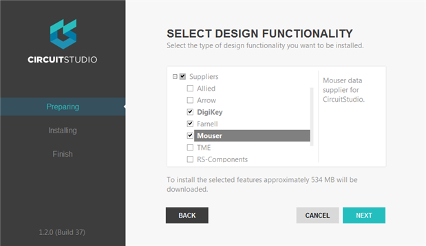
The version I installed was Version 1.2.0 Build 37. While version 1.3 has been announced by Altium, it is not accessible to my CS updater as of today. The download was about 500 MB and took about six minutes to download and install. You will need to attend the installation as questions are asked along the way, to include supplier extensions. I choose a few vendors to see how this works in practice.
After installation, I rebooted my machine and this happened:


Hmmm. This doesn’t look good. I rebooted again and it ran fine. While using AD at work about two years ago, I experienced the “dxp.exe has stopped working” while working on a massive design, and it isn’t fun to wonder if your whole project file was just corrupted - even with daily backups of the design files. I have not experienced any crashes in CS since this one time right after installation of the trial and it seems to be running just fine since.
When you first run CS, you are greeted with a page that is populated with CS news. Notice the trial banner at the top of the frame obscures some items behind it.

A QUICK LOOK AROUND
I clicked the “Start a new PCB Project” and was surprised to see a wizard that offers several PCB standard sizes, such as PCI, AT, XT, PC-104, PCMCIA, S-BUS, VME and a blank PCB. This was nice to see and it’d be great to see hobbyist sized boards (wonder if I can make my own?) that fit enclosures or “sick of beige” offerings. I chose a blank PCB project with the “Create Project Folder” checked.
This creates a project folder in the navigator pane on the left side, which is empty. It’d be nice if the wizard would create the first schematic and PCB files along the thinking of “make the common case the fastest/easiest.”
This is where experience with AD helped me. A quick right click on the project folder and I can “Add new file to project” and an empty schematic sheet is ready to go. You may as well go ahead and add a PCB file now too as you’ll need it later.
I don’t intend for this to be a tutorial on schematic capture and PCB layout/design, so this review won’t be step by step. It is easy to find tutorials online, but I’ll point things that I felt would be tripping points for new users.
ANOTHER INSTALLATION
My job requires travel for time to time and I had two trips during this review, so I installed the actual license on my laptop. It has a Core i7 2.3 GHz processor, 8 GB of RAM, with an SSD running Win7 64 bit. The screen resolution is 1366x768. This fact came into play when one dialog screen was too large to fit the screen vertically.
When I received the email from Altium with the license information, I created an Altium account with the same email address. The installation went fine with no errors at all. This CS install was the same version and build as I installed on my desktop. The install time was also about six minutes.
When I ran it the first time, it worked fine and showed my valid license. To be clear, I was connected to the internet during the whole install process and first run.
A few days later, I had to travel for work. So I planned to explore CS during the flight by looking at the included reference designs without internet connectivity. When I ran CS, it had some typical “website not found” errors, but I was able to use it within expected limitations. When I checked my account from the home page of CS and it confirmed my account was still active.
The limitations when offline include such things as supplier links and the Altium vault not working. The news on the home page was not populated. Probably the biggest limitation I ran into was the lack of help. Apparently, the help system is provided via Internet. The point though is: it is very usable without an Internet connection. I was able to work schematics capture on the flight and save them.
By the way, the files that are saved or generated are saved to the local machine in a manner similar to AD. The generated files usually go into the project outputs within the project folder and with schematics and PcbDoc files are in the project folder itself. I usually try to keep my libraries in the project folder with copies saved off to a common library folder for reuse in future designs.
SCHEMATICS CAPTURE
I found the user interface easy to navigate and most of what I needed was readily available on the ribbon menu. My first design was a very simple one with a two-pin battery connector, a switch, a resistor and two LEDs in parallel. I used one SMD LED and one through hole. Finding a good SMD LED footprint was a challenge and I will probably need to make my own eventually to ensure the LEDs are populated on the board properly. I want a clear mark of the cathode and wasn’t really happy with any of the existing ones I found. I added a silkscreen label to do this, but it’d be nice to have it as part of the footprint.
Some tips for schematics capture that I’ll share. Set your grid to no less than 5. If you go to 1, you run the risk of wires that appear to be connected, but are not. Use netlabels on your key nets, such as Vcc, important signal lines, and differential pairs. This will let you establish net class rules that can do things such as make traces wider. Putting parts can be tedious, especially in CS since it does not have the Parameter Manager tool that AD has. It will be best to send time on the first resistor to make it correct – manufacturer, MFN PN, value, supplier, Supplier PN, etc. Then copy and paste this part for each instance. Be carefully if you change something, such as value, that you update the other info. AD's parameter manager tool can show all of the parts contained in a design in a table format which allows quick changes to footprints, values, comments, etc without having to click on each part individually. I didn't find a comparable tool in CS, but that is an understandable tradeoff, AD is the tool for professional level designs with thousands of parts.
Another tip is when placing your parts, leave the reference designators a R?, C?, U?, etc. Then when you are done placing parts, go to the Tools tab, select the Annotate drop down button and select “Annotate schematics quietly” option. CS will then replace the ? in the reference designator with a unique number so you have R1, R2, C1, U1 and so on automatically. And yes, there is back annotate later for those who want to know now.
I tried to use the Vault, but was frustrated by its lack of relevant results and slow speed, so I left the vault for later in the review.
When schematics capture is complete, you should verify your schematics are good and error free. There are a few tools to help you do this. These include the Electrical Rules Check (ERC), single pin net check and a netlist check. Below is a screenshot of a very simple schematic I threw together to look at links to different footprints (the LEDs), the ability to add notes and general functionality of the UI.

First, is the Electrical Rules Check (ERC) which looks for things like shorts (Vcc to Gnd), floating pins, no driving source, diff pairs that are missing their pair mate, etc. Running the ERC is as easy as going to the outputs tab and clicking on the Electrical Rule Check button. This will give a list of Warnings, Errors and Fatal Errors. Configuring these responses can be done the results tab, or by going into the Project Tab and clicking on the “Generate Outputs” button. If there is a specific error that you are OK with, but don’t want to reconfigure the ERC to ignore this type of error, you can place a “Generic no ERC” directive in the schematic at the location of the error you wish to ignore. This is often used on pins that are intentionally left floating, such as no connect pins on ICs. Look for the “Generic no ERC” in the directives drop down box.
These screenshots are from Project -> Generate Outputs -> Electrical Rules Check -> Configure

The screenshot below is the default configuration, I added more warnings to match my preferences later. Clicking on the colored boxes cycles through the options for each combination.

The second tool is the “Report Single Pin Nets” button on the Outputs Tab to look for nets that are not connected. However, even with some intentional single pin nets, all I got out of this was an empty report. Look for the .REP report file in the Project Outputs folder. Or click on it in the project navigator pane. You can also open this in a text editor.
The third tool is a manual check between a generated netlist and the schematics. However, I don’t see a way to generate this report from the schematics capture phase. I was able to generate it in the PCB phase, but if you’re going to manually do a netlist check against the schematics, you should do this before you place and route the parts on the board.
LIBRARIES
In preparation for the RoadTest, I realized that I wanted to import some of the libraries I made in AD for use with CS. I read that CS cannot use the SchLib and PCBLib files that AD uses, but Integrated Libraries (IntLib) are usable in both. However, I found that CS will read SchLib and PCBLib files. I successfully re-used my AD libs in CS. Perhaps Altium needs to update the CS marketing materials to reflect the latest state of CS as they add features. This is really important as it adds the ability to use third party libraries originally made for AD.
Since this is not a tutorial on libraries and those are available online, I won’t go through the process here. However, I did notice a few things about libraries in CS.
First, there is no wizard to help make footprints. The IPC compliant wizard in AD is nice for parts that have rows of pads, such as SSOP parts. Hopefully you can find good footprints in third party libraries, otherwise you’ll have to place each pad individually.
Speaking of third party libraries, there is a wealth of these available from a list of manufacturers on Altium’s website. You’ll need your Altium account login. I have used some of these with good success. However, I have found that I usually pair the manufacturer’s footprint (PCBLib) with my own SchLib. The schematic library goes together fast and I can edit it for my pin labels and pin grouping as I want.
Below is a SchLib I created for a Microchip PIC18F24K50 that is paired to Microchip’s provided PCBLib.

While making a PCBLib for an ICSP connection, I found I was able to add a triangle marker on Pin 1 of the footprint by using the solid region tool on the Home tab of the ribbon menu. I don’t remember this in AD, but it may be present in the most recent release of AD as well. Below is a screenshot of the pin one triangle marker in the footprint. I added it to both the top and bottom overlays (silkscreens).

IMPORT DESIGN TO A PCB FILE
After verifying the schematics are good, it is time to import the design to a PCB file. You’ll need a CSPCBdoc in your project folder. Click on that and the ribbon menu changes. On the home tab, select the project drop down button and select “Import changes from yourprojectname.PrjPcb.” This will start the Engineering Change Order (ECO) process.
The list should include every part and every net to add to the PCB. You’ll need to press the “Validate Changes” button first. It is very likely you’ll run into errors of unknown pin for lines of “Add Pins to Net” items or “Add Component Class Members”. This is because the parts aren’t added yet; they’re listed above in the ECO list. The next step is to click the “Execute Changes” button which often works 100% as parts are added first and they exist when the pins get added to nets and the components exist when add as component class members. If not, running ECO a second time has always fixed the problem for me in AD.
The ECO process is something that seems like it can also be streamlined in CS. I think there should be a button on the schematic page to export the design in its current state to the PCB file. Now you’ll have a bunch of parts connected in a “rat’s nest.”
NETLIST CHECK
To export the netlist check, while the CSPcbDoc is selected, go to the Tools tab, click on the netlist dropdown and select “Export Netlist from PCB…” It will ask for a confirmation and then open the report within CS. The generated file is placed in the project folder (not the project outputs folder) and can also be viewed / edited by any text editor.

Some things to notice about the Netlist file. It is lacking some things that I remember in AD. Mainly, the format of the file. There are no headers to distinguish between parts and nets and there seems to be a lot of blank lines included. However, it isn’t hard to figure out the parts are marked with square brackets [] and the nets are marked with parentheses (). If you look closely at the netlist file below (which scrolled down towards the bottom of the file), you can see two parts: P1 and D2 followed by the GND net. The GND net shows connection from P1 pin 2 to D2 pin 2. This is not correct as D1 pin 2 should be connected as well. The netlist continues below with the net name followed by the reference designator and pin that is connected to the net. You can see that there are four pins connected to NetP1_1. In really large designs, it is common to see hundreds or thousands of entries on the GND net!

DESIGN RULES
Now; before routing, is when you want to set the design rules for the PCB. While the CSPcbDoc is selected, go to the Home tab and click on Design Rules. Here is where you’ll set your minimum, preferred and maximum sizes for trace widths, vias, trace separations and other design aspects that will need to meet the fabricator’s requirements (such as OSHPark) and your preferences. The screen shot below shows the clearances settings.

I added a design rule to make the power traces 20 mil wide (twice the default width). The easiest way to change these values is to click on teh numbers in the image (such as the 10 mil minimum clearance shown above).
Looking at the figure above, under the top "Width" entry, I added a new rule, named it Width_VCC and configured it to the screenshot below. The next step is to set the priority of this rule above the generic rule which allows all traces to be 10 mil wide. Otherwise, CS will allow all traces to be 10 mil wide and this rule will have no effect. Do this by clicking the priorities button.

ROUTING
After placing the parts on the PCB and editing the PCB shape (easiest way is to use Edit Board Shape on the Home tab), it is time to route.
I tried the autorouter on all of the designs I made during the review. None of the results were completely satisfactory, but that is typical of autorouters to require some clean up afterwards. I found it worked best on designs that had some room between parts to work. On other designs that were more compact the results tended to be ugly for such small designs, so I unrouted all of the nets and used the interactive routing, which I liked and yielded results I was happier with.
There is no ability to export a DSN file to use an external router.
One strange result from the autorouter I noticed was on a board that had a pad configured as a slot. The autorouter placed a trace right through (over) the cutout of the slot. I haven’t resolved that yet and will go back and look at it closer.
RUN DRC
After running the DRC, a dialog box comes up with all of the design rule errors. Another caution: running the Design Rule Check on the Project Tab -> generate outputs will generate a file that goes into the project outputs folder. Will state “passed” when the file is generated – EVEN IF THE FILE CONTAINS RULE VIOLATIONS. The screen shot below shows “passed” but the successfully generated file contained 40 rule violations. So, a caution to the user. By the way, running Run Design Rule Check from the Home Tab (when the PcbDoc file is active) will immediately show a dialog box with all rule violations.

PRINT OUT THE PCB AT 100%
The whole point of using PCB design software is to reduce the time, effort and errors in a PCB before going to a fabricator. Along those lines, another step to help verify the PCB is to print the PCB at 100% and place the parts (don’t forget ESD measures) on the printout to help identify factors that will result in a useless board.
In CS, it is as easy as going to the Outputs tab (CSPcbDoc active) and selecting the Print dropbox. Make sure the settings are configured for 100% printout. This technique is really good at verifying connector footprints are correct and there is enough room around them to use them properly and access connector releases. Some PCB designers place every part on the printout to verify all footprints are correct.
LET’S GO TO FAB
Generating Gerber and NC Drill files is ridiculously easy compared to AD. There are buttons on the Outputs tab for each that will take you through the configuration and file generation.
Here are the steps I used to generate files to go to OSHPark.
On the Outputs tab, click Gerber – then on general tab change format to 2:4

No I used the outline layer for the board outline. In the past, I have used the KeepOut layer in AD for this, but have found out some footprints have Keepout features in them to keep an autorouter from placing traces where they shouldn’t go. In order to eliminate problems with the fab possibly putting holes in the PCB I don’t want, I used the outline layer.
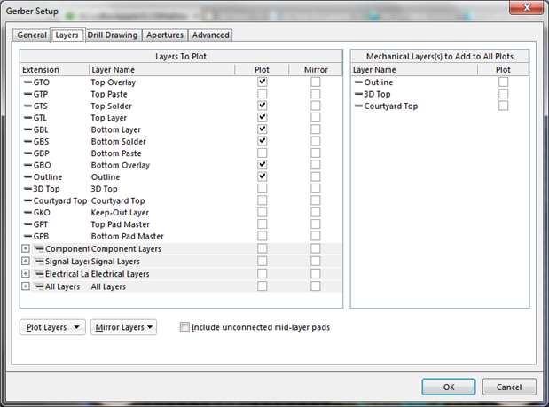
The Drill Drawing and Apertures is unchanged. On the Advanced tab: change keep leading zeros and ref to absolute zero (note: I did not move the origin of the PCB in the CSPCBDoc file).

This will generate the Gerbers and put them in the Project Outputs folder.
Now to generate the NC Drill file. You’ll need to make similar changes, but they are all on one page:
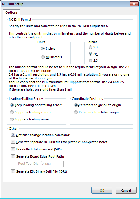
The NC Drill file output is a .txt file in the Project Outputs folder. In order to upload to OSHPark, you’ll need to rename this from TXT to XLN (in your OS file manager) and then rename the Outline file from .Outline to .GKO. Then zip these eight files together: .GBL, .GBO, .GBS, .GKO, .GTL, .GTO, .GTS, .XLN. Note that four layer boards will have two more layers to generate (G1 and G2 in CS).
Now you can upload the file to OSHPark, go through their process, look at each layer OSHPark shows as one last check and then submit your order. In about two weeks, you’ll have three purple boards for each design ordered and probably a sticker too!
In the net few days, I will add a guide that explains how to setup CS for use with OSHPark as a separate document.
AN IMPORTANT NOTE – UNDOCUMENTED FEATURE?
I noticed that generating Gerbers and NC drill files from the Outputs tab works fine, but is not the only way to get these files. The other way is to go to the Project Tab and click Generate Outputs. The caution is that these files have their own configuration, which, even though they look the same as above, are NOT configured the same even after the changes are made as shown above. The risk is using a different method to generate Gerbers and have the resulting files turn out different.
3D VIEWS
The 3D PCB viewer is limited to just a few viewpoints. Two top down views (or bottom views) and one “Orthogonal rotation” view. I could not figure out a way to rotate the board – I doubt CS allows this, but I could pan and zoom.

AD and CS
I was very pleasantly surprised to see that CS will open AD’s SchDoc files. Having these schematic files open in CS is a big time saver. There are two things to be aware of. First, you’ll need to re-establish the library links to the SchLib and PCBLib files. Second, the PCB file from AD will not open in CS. So, you’ll need to place and route the whole thing again. It is better than starting from ground zero, but a bit disappointing. A simple PCB change for a design done in AD will require some effort and risk to build a new PCB file in CS.
VAULT
Since Altium makes a big deal of the Altium Vault, I decided to try it out and see what was in it. But at first, I couldn’t find the Vault on the menu ribbon. Using the search box at the top right of the screen, it took me straight to the setting to enable access to the Vault (hmm, wonder why that wasn’t on by default?).
After enabling it, I was able to access the Vault panel. Note that the Vault is accessible from the File drop down menu.

One of the simple designs I built was a adapter board for a Microchip ICD3 or RealICE to work with demo boards that use the 6 pin Pickit3 header. I had a part identified for the 6p6c RJ12 connector, but could not find a footprint anywhere, so I searched for 54601 (no hits), and 6p6c (no hits) in the Vault. I was wondering if I did something wrong. I noticed a search tab at the bottom of the screen and tried that. Also no hits. So I searched for 18F on the search tab (with “Generic Search” shown) and again no hits. This is odd since Microchip makes numerous 18F parts. Going back to the “Structure” tab of Vault, 18F returned a handful of parts.
Later, I tried a search for PIC18F45K22 and got the result below. The complete part numbers are impossible to read as they are too long. This was on my laptop with the 1366 pixel wide screen. I found the best way to find parts was to look in the structure tab (at the bottom), look by manufacturer, and then look in the correct sub category for parts.

Placing parts took some trial and error. Here is an example using TE Connectivity’s HTU21, which can be found by searching HTU21. The screenshot below shows the SCH symbols highlighted, but I found the best chance of placing parts is by clicking on the sub-category (in this case “No Category”) and then right-clicking on the item revision number as shown below. This took me back to the schematics page to place the symbol. The footprint was already associated when I imported the change to the PCB and it looked good.

I feel if I can find a part in the Vault I may use it. I’m concerned of the implications of the Vault's need to be online to work. What if I need to work on the design while offline? What if my subscription to the Vault has expired? Is it possible to save Vault parts to local library file? I'll look into this make a blog post with my experiences.
SUPPLIER LINKS
I like the supplier links feature. When placing a part on the schematics page, right click the symbol and click on Supplier links. Click Add. Then put a part number in the search window. Here, it is better to start with a very specific part number since only 12 results are shown a time. See the screenshot below for the HTU21. Notice Digi-Key has two entries. I had to look at the more detailed view at the bottom right to find the difference between the two parts. Clicking on one adds a lot of detailed information to the schematic symbol properties, allows the part number to show up on the schematic and also in the generated Bill of Materials (BOM). This is only distributor information, no schematic symbols or footprints here, but it is really handy and I plan to use this on all designs going forward.

BOM GENERATION
The ability to have a complete Bill of Materials for the design is important. It took me a while to find where the BOM generation is at in CS and happily, it is in there.
Go to the Project Tab and click on Generate Outputs. The BOM is the top line. Click on configure to get something like the screen shot below. This shows a preview of the first few lines of the BOM and allows you to tailor the final output. Notice this design has supplier link information which shows up under “Solution 1”. One of those hard-to-figure-out-things is how to sort the results by Manufacturer PN. Notice in the list below, C1, C3 and C4 are different than C2. But in the default configuration, these all who up on the same line. In order to sort by PN, you need to drag the column name from the bottom left of the screen to the “Grouped Columns” area.
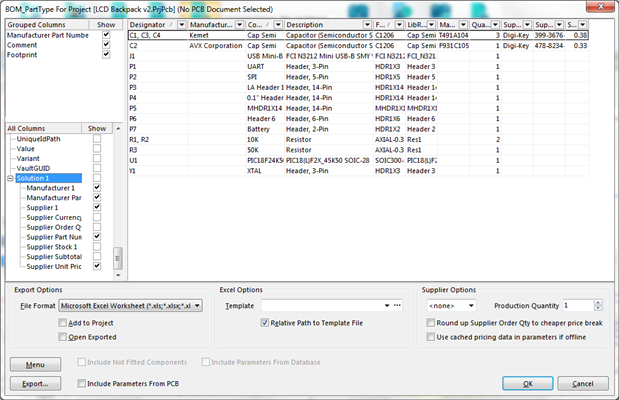
To generate the BOM here, click export at the bottom left. Clicking OK saves the configuration.
ROOM FOR IMPROVEMENT
Here are some things I'd like to see Altium address in a future release.
ANSWERS TO SPECIFIC QUESTIONS ASKED AT THE START OF THE REVIEW
I have added answers inline below. These are based on my experience with Circuit Studio Version 1.2
1. Explore the ability to change the Electrical Rule Check (ERC) settings. I recall adjusting these in Altium Designer (AD) to reduce the amount of ERCs and I wonder if these become annoying with Circuit Studio (CS)?
It looked similar to the configuration screen in AD to me. I was able to add more warnings to match my preferences. I covered this in my review.
2. One I'm REALLY interested in: Evaluate and share the experience of the process of creating a new part footprint - particularly one with unique features, like a connector with thru-hole mounts. I see that CS does not have the footprint wizard that AD has. I wonder about the user experience to create footprints in CS?
There is no footprint wizard which I recall was really useful for parts that have rows of pins, such as SSOP.
There is an ability to add images (simple B&W works best) and for “solid regions” which I used to make simple geometric shapes.
3. It appears CS doesn't have the ability to export to the Specctra external router. I would like an investigation to see if the free Elektra router or the Freerouting.net router will work or is the ability to generate DSN files missing entirely? If this ability is missing, I'm curious about the quality of the internal router. I would run a design I routed in AD and see how well CS does with it.
There is no ability in CS to export a DSN file to external routers.
4. I've used AD and I'm wondering what is the difference in CS's "basic" pad stackup versus the "full" one in AD?
I didn’t notice anything missing or different from what I remember in AD14.
5. The referenced document also says non-circular holes are not supported. What about slots?
A pad has an easy way to become a slot (simple check box to enable), but I did not send a design to fab with a slot.
I also noticed a problem where the autorouter placed a trace over the slot. I’m still looking at this.
6. I am disappointed the touch component support is missing, but I suspect that is not a big deal if it is easy to create our own footprints easily (see #2).
I think the easiest way to get chevrons or wagon wheels for touch pads will be to use a third party library, or to make one in something like paint.net and then import the image.
7. Altium states Cs has a reduced Design Rule Check (DRC) capabilities compared to AD. Are there any problems suspected or noted with passing DRC to get the boards made?
I didn’t see any reduced DRC capabilities in CS. I think some of the earlier marketing material for CS may be out of date as they have added capabilities.
No fab issues with the three different designs I sent to fab.
8. I a, curious about library management, the ability to create my own libraries, store them locally, as well as CS's ability to "consume Vault content." What does that mean in practice?
The ability to use SchLib, PcbLib and IntLib files is there. Locally created and stored files are the norm.
I’m still looking at the Vault – particularly the ability to bring Vault content into a local library.
9. I have had AD crash albeit infrequently and on very large designs, but was saved from serious loss by my backup system. Do the reviewers experience any stability issues?
I only had one crash and that was during the first run after installation of the trial.
A reboot of the system and it has worked fine since.
On my laptop, I installed CS (same version) with the one year license and it had no problems at all.
I did most of the review on my laptop.
10. While I don't use Eagle, I suspect there are those who are interested in the ability and the experience of importing an Eagle (or other tool's) design. Along those lines, I'd like details on how well this import is accomplished? For example, I'd like to know if net classes and if net class specific design rules are maintained. In AD, I can set a 3P3V net class along with a design rule that all nets in 3P3V should be 15 mils wide, whereas other traces may be 10 mils wide. I've noticed that designs I have exported in AD and then import into other tools lose these design aspects.
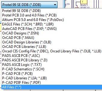
This screenshot shows the file types CS will import. I did not test any of them.
I was able to open AD14 SchDoc files (yeah!) but there is no way to open AD PcbDoc files.
Net class specific design rules were lost.
I have not tried to import designs from other products, but I can do this if anyone wants me to try.
11. I see step export of the final PCB design is not included in CS, but I am curious about its ability to render the board in 3D and that reviewer's experience with that.
The 3D viewer is present, but gimped. There are really two options to view the board.
Directly down (top or bottom, option to rotate), or one fixed orthogonal view.
12. Of course, I hope the reviewers take designs from schematics capture all the way through production of PCBs (at least one design if not more).
I worked on at least six designs of varying complexity. The most complex has four layers, with a ground plane pour on the second layer, differential pair traces, and contains about 30 components.
Some designs were entirely new, some were imports of AD designs.
I sent three designs off to fab and the boards came out fine.
Below (L) is one of the very simple designs I made - an adapter to use a Microchip ICD3 on a development board that has a Pickit3 interface.
To the right is the populated board plugged into a Curiosity board for testing.


THE SCORE
The two biggest areas I deducted points from CS for were price and "demo was easy to use", which I interpreted as the quality of relevant support materials.
As for price, Let’s look at what you get for $1,000 compared to other tools. Diptrace full is $1,200. Eagle Ultimate is $1,600 for 16 layers and you have to deal with that awful UI and library management. The version of Target 3001! that has at least the same level of capability is $3,400. Of course, Kicad is free…
I wish Altium would release levels of AD similar to other tools. A structured approach by component count, layers, routing space,etc. I think if CS had a version that was limited to four layers, maybe six inch square board size and sold for a competitive price, I think they'd capture more market share of the hobbyist / budding professionals and pull them into the Altium product line.
The support materials are plentiful. There are videos and documents on element14 and Altium's website (particularly for AD, but often you can figure out what you need). However, I did find CS marketing materials are out of date with incorrect information that may dissuade potential users who are looking for specific features.
Finally, you need to be aware that if you bring designs into Altium; especially CS, it is hard to impossible to get them out to use in other non-Altium tools. AD has some ability to export.
48/60 = 80%
OVERALL CONCLUSION
Since I have designs, libraries, and experience with Altium Designer, I plan to continue to use CS (since I no longer have AD access through my employer). For someone starting out, the user interface in CS is better than AD, it less daunting than AD and has enough features to satisfy designs that aren’t too complex (thousands of parts).
Altium has announced version 1.3 of CS will be released "soon" and it may address some of the problems I noted.
If you want to get experience with a professional level tool that works offline, allows local storage of design files and shares a lot of functionality with Altium Designer without the cost of AD, CS may be for you. It is worth a download of the trial to give it a try.
Finally, thanks to element14 for providing the software for this review.
I hope you've enjoyed reading this!
Cory


