element14 Community
element14 Community
    Register Log In
  • Site
  • Search
  • Log In Register
  • Community Hub
    Community Hub
    • What's New on element14
    • Feedback and Support
    • Benefits of Membership
    • Personal Blogs
    • Members Area
    • Achievement Levels
  • Learn
    Learn
    • Ask an Expert
    • eBooks
    • element14 presents
    • Learning Center
    • Tech Spotlight
    • STEM Academy
    • Webinars, Training and Events
    • Learning Groups
  • Technologies
    Technologies
    • 3D Printing
    • FPGA
    • Industrial Automation
    • Internet of Things
    • Power & Energy
    • Sensors
    • Technology Groups
  • Challenges & Projects
    Challenges & Projects
    • Design Challenges
    • element14 presents Projects
    • Project14
    • Arduino Projects
    • Raspberry Pi Projects
    • Project Groups
  • Products
    Products
    • Arduino
    • Avnet & Tria Boards Community
    • Dev Tools
    • Manufacturers
    • Multicomp Pro
    • Product Groups
    • Raspberry Pi
    • RoadTests & Reviews
  • About Us
  • Store
    Store
    • Visit Your Store
    • Choose another store...
      • Europe
      •  Austria (German)
      •  Belgium (Dutch, French)
      •  Bulgaria (Bulgarian)
      •  Czech Republic (Czech)
      •  Denmark (Danish)
      •  Estonia (Estonian)
      •  Finland (Finnish)
      •  France (French)
      •  Germany (German)
      •  Hungary (Hungarian)
      •  Ireland
      •  Israel
      •  Italy (Italian)
      •  Latvia (Latvian)
      •  
      •  Lithuania (Lithuanian)
      •  Netherlands (Dutch)
      •  Norway (Norwegian)
      •  Poland (Polish)
      •  Portugal (Portuguese)
      •  Romania (Romanian)
      •  Russia (Russian)
      •  Slovakia (Slovak)
      •  Slovenia (Slovenian)
      •  Spain (Spanish)
      •  Sweden (Swedish)
      •  Switzerland(German, French)
      •  Turkey (Turkish)
      •  United Kingdom
      • Asia Pacific
      •  Australia
      •  China
      •  Hong Kong
      •  India
      • Japan
      •  Korea (Korean)
      •  Malaysia
      •  New Zealand
      •  Philippines
      •  Singapore
      •  Taiwan
      •  Thailand (Thai)
      • Vietnam
      • Americas
      •  Brazil (Portuguese)
      •  Canada
      •  Mexico (Spanish)
      •  United States
      Can't find the country/region you're looking for? Visit our export site or find a local distributor.
  • Translate
  • Profile
  • Settings
Business of Engineering
  • Technologies
  • More
Business of Engineering
Blog Creating a new product - Prototyping
  • Blog
  • Forum
  • Documents
  • Quiz
  • Events
  • Polls
  • Files
  • Members
  • Mentions
  • Sub-Groups
  • Tags
  • More
  • Cancel
  • New
Join Business of Engineering to participate - click to join for free!
  • Share
  • More
  • Cancel
Group Actions
  • Group RSS
  • More
  • Cancel
Engagement
  • Author Author: Workshopshed
  • Date Created: 1 Nov 2014 10:25 PM Date Created
  • Views 1271 views
  • Likes 2 likes
  • Comments 8 comments
  • entrepreneurship
  • business
Related
Recommended

Creating a new product - Prototyping

Workshopshed
Workshopshed
1 Nov 2014

Shortly after writing my last post I read an interesting article from Tom Maiorana on 5 Prototyping lessons from a BMX backflip this is an extension of the Fail Early, Fail Fast, Fail Often principle.


This consists of 5 stages.


  1. Deconstruct the challenge
  2. Minimize risk
  3. Use ignored resources
  4. Remove as much as possible
  5. Maximize cycles of learning


It seemed a good principle to apply to my new board prototype.


Deconstruct the challenge

When you are looking at your product or service, break the whole into all of its different elements. Then focus on the one that is most critical. For those of you familiar with the Lean Start-up, this would be what Eric Reis calls your “leap-of-faith assumption”.


The main steps of my project are:

  1. Design the schematic
  2. Design the PCB layout
  3. Assemble the boards


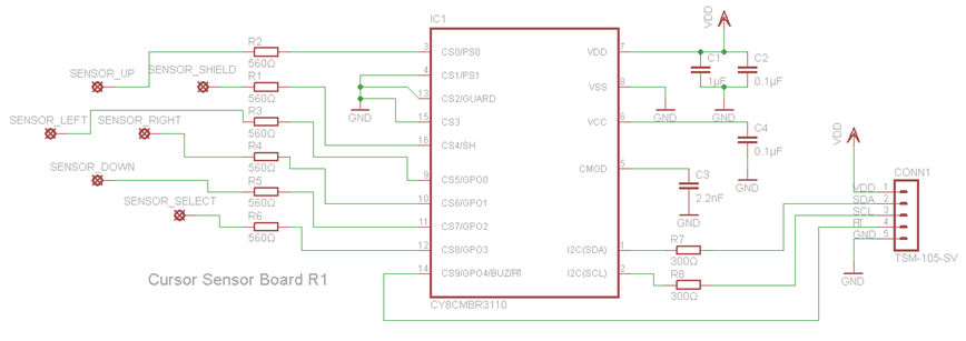
The schematic is effectively straight off the data sheets.

image


Assembly of the boards is something I'll likely need a bit of practice with but the processes for doing this are all fairly well defined, I'll likely hand solder the prototype boards.

This means that the critical step is the design of the PCB layout.


However following on from this is a shift from prototyping to production so it might be worth re-running this process at that point to ensure success.


Minimize risk

As you think about prototyping your offering, brainstorm ways in which you can learn with minimal risk.


For me the key risk is that I'll spend lots lots of time and money and have nothing to show for it. This breaks down into two parts, firstly not purchasing lots of tools up front and making do with what I have. The other risk is having PCBs made and then finding out that they don't actually work. So what can I do to get to a working design quickly without having lots of PCBs made that don't work?


Use ignored resources

Think about the untapped resources that you might have at your disposal? Is there a bored developer who’s looking for an interesting project? A space no one cares about? Find them and put them to use


Looking at the resources I have available I don't have any PCB creation capabilities but I might be able to talk to a local hackerspace and get my boards made that way.


I did think about what I could do before making the PCBs. There's lots of useful information in the CapSenseRegistered Design Guide as well as a spreadsheet that allows you to check your parameters. I did wonder if I could use the design rule checks or a Write an Eagle PCB ULP to validate my design such as checking the trace lengths, separation and routing. However given the size of my board and the max trace lengths (e.g. 50cm) this does not seem like good time spent.

I also found a useful article from Sparkfun - Better PCBs in Eagle which suggests tips for ensuring that boards have good tolerances so that shorted connections are less likely to happen.


Another idea I found from Element14 is Using Paper Protos to Check Footprints this allows me to check that I'll be able to place and solder the components before getting the board made and also that the button layout is sensible.

I could also Render 3D images of PCBs to ensure the board looks ok and use a Gerber Viewer to ensure that the Gerber files are generated as expected.


Several of the PCB houses can run their own Design Rule Checks against your board or provide a rules check settings file to download. I may take advantage of the DRC file provided by Sparkfun for this.


Other resources I can utilise are some of the Element14 members, I've had a offer for someone who wants to take a look at my project.


There are also some free electronic circuit simulators List of free electronics circuit simulators - Wikipedia, the free encyclopedia although I'm not sure how I could utilise these in my project unless I can also simulate the MBR3 chip.


As mentioned in my last post it should be possible to re-use the CapSense evaluation board along with EZ-Click software to test and configure the boards. The MBR3 chip has some onboard diagnostics so it might make sense to write a bit of Arduino code to read these or use the testing tools that come with EZ-Click.


Remove as much as possible

For organizations, this often means your prototypes will have a lot of throw-away work. But you’ll be moving so fast that it’s actually more efficient than a traditional way of working.


For my prototype my first circuit is simply one from the data sheet with the 5 inputs and host interupt. I was wondering if I could make this as a breakout board and have the sensors as a separate board. This might give me a little advantage in that I'd not need to solder the components for each iteration although that might be something I'd want to practice any way. I also wondered if I could create a board with a blank area on it and use conductive paint to draw different pads. However I think these might actually add complexity to the project and doing my iterations on screen electronically might be preferable.


Maximize cycles of learning

As you prototype, think about ways to create an exponential jump in the number of learning cycles.


To maximise my cycles it makes sense to do as many as possible electronically using the above resources before sending the board out for production.

Once I'm happy with the design I can do another set of cycles to get the boards working.


Conclusion

As a process I'm not totally convinced that the BMX Backflip principles can be applied here but I think the process of deconstructing the challenge and reviewing resources has been useful.

  • Sign in to reply

Top Comments

  • Problemchild
    Problemchild over 11 years ago +2
    Good one this is a very interesting post. On these small boards which don't have too small components it would be good to try the baby CNC machines to mill your board shortening your turnaround time..…
  • mcb1
    mcb1 over 11 years ago in reply to Workshopshed +1
    My first boards used paint to lay out the tracks and pads ..... Happily they have not survived as they were nothing nice to look at, but technology has moved on. A long while ago they guys at work made…
  • Workshopshed
    Workshopshed over 11 years ago in reply to Problemchild

    Yes having on-site PCB making capability would make sense for this, I keep coming back to the idea of a breakout board which would allow me to try out different sensor configurations.

    • Cancel
    • Vote Up 0 Vote Down
    • Sign in to reply
    • More
    • Cancel
  • Workshopshed
    Workshopshed over 11 years ago in reply to Problemchild

    Is that a specific technique or just how people do things in New York?

    • Cancel
    • Vote Up 0 Vote Down
    • Sign in to reply
    • More
    • Cancel
  • Problemchild
    Problemchild over 11 years ago

    Good one this is a very interesting post. On these small boards which don't have too small components it would be good to try the baby CNC machines to mill your board shortening your turnaround time... giving you more time to "fail often "

    • Cancel
    • Vote Up +2 Vote Down
    • Sign in to reply
    • More
    • Cancel
  • Problemchild
    Problemchild over 11 years ago in reply to mcb1

    Sounds rather like Manhattan style

    • Cancel
    • Vote Up 0 Vote Down
    • Sign in to reply
    • More
    • Cancel
  • mcb1
    mcb1 over 11 years ago in reply to Workshopshed

    My first boards used paint to lay out the tracks and pads .....

    Happily they have not survived as they were nothing nice to look at, but technology has moved on.


    A long while ago they guys at work made there own pads on pcb by reshaping a large drill bit.

    They removed the centre so that it produced a 'donut' or an isolated pad is a large earth plane.

    It wasn't quite smd since most of the components were in the air, but it did overcome the issues of adjacent track capacitance found in the breadboard/veroboard design.


    Mark

    • Cancel
    • Vote Up +1 Vote Down
    • Sign in to reply
    • More
    • Cancel
>
element14 Community

element14 is the first online community specifically for engineers. Connect with your peers and get expert answers to your questions.

  • Members
  • Learn
  • Technologies
  • Challenges & Projects
  • Products
  • Store
  • About Us
  • Feedback & Support
  • FAQs
  • Terms of Use
  • Privacy Policy
  • Legal and Copyright Notices
  • Sitemap
  • Cookies

An Avnet Company © 2025 Premier Farnell Limited. All Rights Reserved.

Premier Farnell Ltd, registered in England and Wales (no 00876412), registered office: Farnell House, Forge Lane, Leeds LS12 2NE.

ICP 备案号 10220084.

Follow element14

  • X
  • Facebook
  • linkedin
  • YouTube