element14 Community
element14 Community
    Register Log In
  • Site
  • Search
  • Log In Register
  • Community Hub
    Community Hub
    • What's New on element14
    • Feedback and Support
    • Benefits of Membership
    • Personal Blogs
    • Members Area
    • Achievement Levels
  • Learn
    Learn
    • Ask an Expert
    • eBooks
    • element14 presents
    • Learning Center
    • Tech Spotlight
    • STEM Academy
    • Webinars, Training and Events
    • Learning Groups
  • Technologies
    Technologies
    • 3D Printing
    • FPGA
    • Industrial Automation
    • Internet of Things
    • Power & Energy
    • Sensors
    • Technology Groups
  • Challenges & Projects
    Challenges & Projects
    • Design Challenges
    • element14 presents Projects
    • Project14
    • Arduino Projects
    • Raspberry Pi Projects
    • Project Groups
  • Products
    Products
    • Arduino
    • Avnet Boards Community
    • Dev Tools
    • Manufacturers
    • Multicomp Pro
    • Product Groups
    • Raspberry Pi
    • RoadTests & Reviews
  • Store
    Store
    • Visit Your Store
    • Choose another store...
      • Europe
      •  Austria (German)
      •  Belgium (Dutch, French)
      •  Bulgaria (Bulgarian)
      •  Czech Republic (Czech)
      •  Denmark (Danish)
      •  Estonia (Estonian)
      •  Finland (Finnish)
      •  France (French)
      •  Germany (German)
      •  Hungary (Hungarian)
      •  Ireland
      •  Israel
      •  Italy (Italian)
      •  Latvia (Latvian)
      •  
      •  Lithuania (Lithuanian)
      •  Netherlands (Dutch)
      •  Norway (Norwegian)
      •  Poland (Polish)
      •  Portugal (Portuguese)
      •  Romania (Romanian)
      •  Russia (Russian)
      •  Slovakia (Slovak)
      •  Slovenia (Slovenian)
      •  Spain (Spanish)
      •  Sweden (Swedish)
      •  Switzerland(German, French)
      •  Turkey (Turkish)
      •  United Kingdom
      • Asia Pacific
      •  Australia
      •  China
      •  Hong Kong
      •  India
      •  Korea (Korean)
      •  Malaysia
      •  New Zealand
      •  Philippines
      •  Singapore
      •  Taiwan
      •  Thailand (Thai)
      • Americas
      •  Brazil (Portuguese)
      •  Canada
      •  Mexico (Spanish)
      •  United States
      Can't find the country/region you're looking for? Visit our export site or find a local distributor.
  • Translate
  • Profile
  • Settings
Embedded and Microcontrollers
  • Technologies
  • More
Embedded and Microcontrollers
Blog Renesas RX65 Envision Kit - part 12: RAM Use with GCC ToolChain
  • Blog
  • Forum
  • Documents
  • Quiz
  • Polls
  • Files
  • Members
  • Mentions
  • Sub-Groups
  • Tags
  • More
  • Cancel
  • New
Embedded and Microcontrollers requires membership for participation - click to join
  • Share
  • More
  • Cancel
Group Actions
  • Group RSS
  • More
  • Cancel
Engagement
  • Author Author: Jan Cumps
  • Date Created: 3 Jan 2020 5:46 PM Date Created
  • Views 2892 views
  • Likes 6 likes
  • Comments 14 comments
  • rx65n
  • gcc
  • renesas
  • linker
Related
Recommended

Renesas RX65 Envision Kit - part 12: RAM Use with GCC ToolChain

Jan Cumps
Jan Cumps
3 Jan 2020

Goal: This post tries to explain what objects are placed where in RAM when using the GCC toolchain.

It's intended as self-documentation. When using the LCD, you need large continuous chunks of memory for the frame buffers.

Memory is limited on controllers. Continuous large blocks even more so.

To be able to reserve these buffers, it's useful to understand where the linker places code, data, stacks and housekeeping blocks.

Knowing their position and size - and knowing if you can move things without side effects - are the hooks to eek out maximum available memory for buffers and custom logic.

image

Not a goal of this post:  Explain the non-RAM ranges or how to try and save data or code size during development.


RX65N RAM


The controller has two RAM ranges.


on-chip RAMSize (bytes)Start addressEnd address
Standard RAM

0x00040000 / 262144

0x000000000x0003FFFF
Expansion RAM

0x00060000 / 393216

0x008000000x0085FFFF
Total RAM0x000A0000 / 655360


The first range is available on all RX65N devices. The Expansion RAM is dependent on the particular device.

The R5F565NEDDFB on the Envision kit has the full 640K.

image

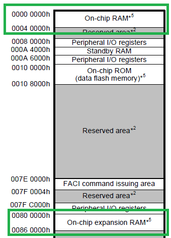
source: ammended memory map from the Renesas RX65N datasheet


640K is plenty. However, because the memory is not continuous, reserving two 130560130560 blocks (the buffer size for a 480 wide * 272 high * 2 bytes for colour) will need proper care.

It's not a desperate situation image - 2 blocks fit in the expansion RAM. But for a larger display, they wouldn't.


What Goes to RAM


The objects that will go to RAM are:

  • the start address and top pointer of the heap
  • the two stacks (istack for interrupts, ustack for user)
  • data (yours and that from linked in libraries)
  • Dynamically allocated memory will go to the heap. The heap in this controller is of a fixed size in this RAM region and grows up towards its tail.


image

image: the Smart Configurator in e2 studio: define the istack, ustack and heap sizes


The linker command file and related assembler file generated by the project wizard and the Smart Configurator place all of that in the Standard RAM area.


The Linker Memory Areas


The GCC linker command file is where you define what is placed where by the link and load process.

You define what blocks of memory are available, where they are located and the size (if your controller supports it, also if you can read/write/execute in that area). You can also use it to define blocks that aren't available.

Then you define what parts of your code go to those areas.

Typically, you have memory regions, output + input sections and assignments.

  • region: an area of memory. It has address and size.
  • output section: a container that can be filled with code or data, and that's placed within a region, either at the next available address or at a fixed point
  • input section: a named container, belonging to an output section, where that GCC toolchain assign code and data to. It's complex image but your variables and code will be assigned to a particular input section.
    Input sections are then placed within the output section they are assigned to.

You could think of input sections as data that's inputted (gathered) into the output section. The output sections are then outputted (placed) to memory regions.

Assignments are labels that are internally used by the toolchain, but also available to you if you want to assign a memory area to a particular address without hardcoding that address in your code.


For our controller, the memory areas are:

image

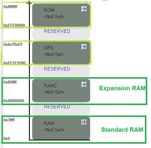
image: The 4 ranges defined in the linker file


I'm ignoring OFS and ROM in this post. (just for info: your code goes to ROM (flash) and is executed from there)

The RAM and RAM2 blocks are the standard and expansion RAM. This is our focus.

note: the loader file generated by e2 studio's project wizard has a bug. It places expansion ram on ox0008000 instead of 0x00800000. Fix that manually after generating a project.


View What's Where in RAM


Eclipse has a graphical editor that helps you lay out the memory and its use. That includes a graphic overview of the memory.


image

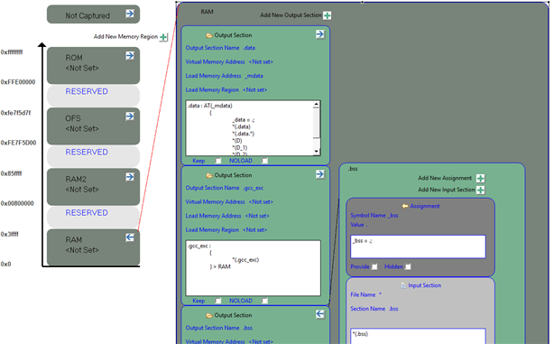
image: the Eclipse linker file viewer


That will give you an overview of how the linker will place objects. What it will not show is the complete picture with the stacks allocated.

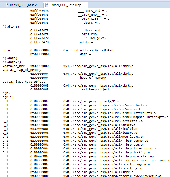
To see that, you can use the GCC linker's map file, and the handy AMAP viewer.


image

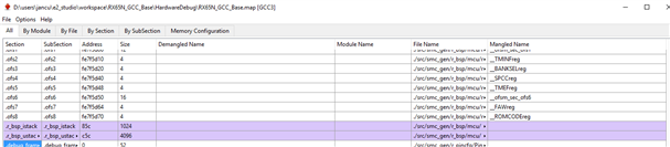
image: AMAP viewer showing the sections in a Renesas RX65N GCC map file


The map file is generated during the build process, so you need a compilable program (I just created a empty Renesas C program for the GCC toolchain, with Smart Configurator support).

The advantage is that it has factual data about how much space is taken by runtime library data, stacks, data, and their exact locations.


Objects Placed in RAM


As seen earlier, all objects that go to RAM are placed in the standard RAM area by the default linker script. RAM2 is not used by default. So the linker will not place anything in expansion RAM.

The standard RAM region has a number of output sections. Some consecutive, some at a fixed address:

image

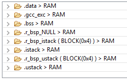
image: output sections assigned to standard RAM


The tree board startup sections (r_bsp_*) are placed on fixed addresses. All the rest are placed where the linker sees fit within the RAM region.

A good explanation is available from wikipedia.

  • .data contains initialised global and static variables, and the heap start and end points.
  • .gcc_exec contains nothing
  • .bss contains the uninitialised global and static variables and the heap.
  • the stacks contain values pushed on the stack, such as parameters and variables declared within a function.
    They have a fixed size set in the startup assembler code. They are set to NOLOAD so won't be initialised.
  • .r_bsp_NULL, I believe is used for the board upbring code. It reserves 100 bytes.
    For some reason it's not visible in the AMAP viewer but it's the area between end of .bss and start of the stacks. It's content is copied from a ROM address at startup.


For a program built without debug information, yet without optimisation, here's the content of the RAM region:


image

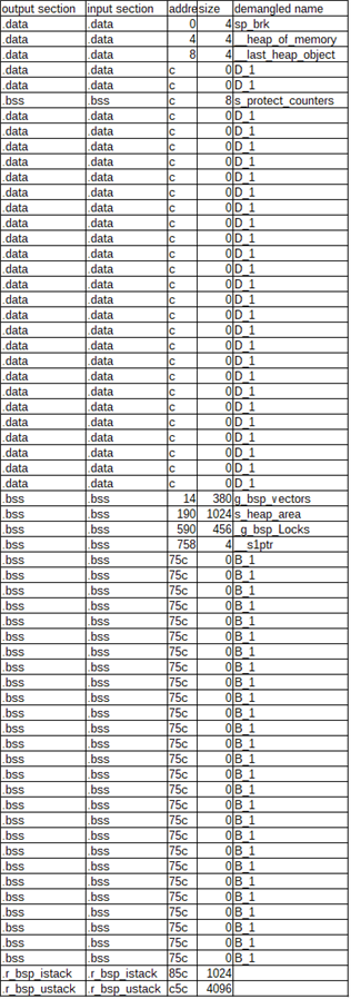
image: extract from the AMAP tool showing RAM region objects.


I did a first attempt in fixing LCD buffers at a fixed free spot in Renesas RX65 Envision Kit - part 10: Reserve LCD Frame Buffer in Expansion RAM with GCC.

That was done with the knowledge that the expansion RAM was unused.

With the info of this post at hand, I should be able to come up with a good strategy to allocate buffers for the LCD display in standard RAM too...

  • Sign in to reply

Top Comments

  • Andrew J
    Andrew J over 5 years ago +2
    For the LCD ram buffers, it’s worth bearing in mind that when using emWin, you will want two of these buffers (i.e. 2 x 261,120 bytes) to operate the screen without flickering, depending upon the frequency…
  • Jan Cumps
    Jan Cumps over 5 years ago +1
    Eclipse has a reasonable good map viewer too: You can open it via Window -> Show View -> Other -> Memory usage. It 'll load the map file of the currently active build configuration. A particularly useful…
  • Jan Cumps
    Jan Cumps over 5 years ago in reply to Andrew J +1
    Andrew J wrote: For the LCD ram buffers, it’s worth bearing in mind that when using emWin, you will want two of these buffers (i.e. 2 x 261,120 bytes) to operate the screen without flickering, ... Did…
  • Andrew J
    Andrew J over 5 years ago in reply to Jan Cumps

    I did post to the emWin forum a couple of times and got some useful responses so it might be worth asking.

    • Cancel
    • Vote Up +1 Vote Down
    • Sign in to reply
    • More
    • Cancel
  • Jan Cumps
    Jan Cumps over 5 years ago in reply to clem57

    clem57  wrote:


    Just a thought here: Where are the interrupt vectors? They usually go in a fixed location

    It looks like the interrupt table is not fixed in this controller. There's a register pointing at it's location.

    If the address below 0x00000100 is used, it's magical, because no code or linker info points to it.


    This one makes me worried, it's in the binary emWin library:

    image

    But I'm unsure if it's really an issue, because the library code may get relocated by the linker. (although all other objects of the emWin lib are pointing to ROM ...

    the .rodata segment is the ROM (flash) region. Not sure why it show this part of the library there. I don't have the source so it's a wild guess.

    • Cancel
    • Vote Up 0 Vote Down
    • Sign in to reply
    • More
    • Cancel
  • clem57
    clem57 over 5 years ago in reply to Jan Cumps

    Just a thought here: Where are the interrupt vectors? They usually go in a fixed location

    • Cancel
    • Vote Up 0 Vote Down
    • Sign in to reply
    • More
    • Cancel
  • DAB
    DAB over 5 years ago

    It has been a long time since I did this level of detailed work in assembly language.

    Memory mapping was very key in the old days as few of us had a fully populated memory space in which to do our software.


    DAB

    • Cancel
    • Vote Up +1 Vote Down
    • Sign in to reply
    • More
    • Cancel
  • Andrew J
    Andrew J over 5 years ago in reply to Jan Cumps

    The versions of the emWin config files are specifically for the RX65N I believe: it could be that they are specific for the CC-RX compiler as well.  There's nothing to say there isn't a bug in them either - is this the version you got from me when I created a base emWin build?  I had an issue initially, if you recall, getting my original build to work and I gave up and took someone else's copy which did work (from the forum) - that's the version you took and which I had no subsequent problems through all my testing. If there are bugs, I never uncovered any.  Later, I figured it out what my original problem was: the linker was using incorrect memory allocation and changing it allowed my build to work.  It may be that you need to comb through the files in emWin "Config" directory to check that entries match what you need.


    If you need any project files from me let me know and I'll post it up - actually, there should be a full set in my final post, zipped up.  You may still be able to use the CC-RX to check it out but they're only text/XML files.  The project won't run for you of course because you won't have the components to reproduce on a breadboard but you could still look through the linker configuration.


    "The only line to change in LCDConf.c should be that #define to set the number of buffers."

    I say this as I believe there is standard code in LCDConf.c to use that definition - either 1, 2 or 3 (3 is the max but I doubt there is the RAM for this many), bounded with statements like "#if (NUM_BUFFERS == 2)" - but you could check just to make sure.  In any case, using multiple buffers is useful for screen refresh but not strictly necessary, certainly not for your testing.  You could turn it off (set to 1) initially.

    • Cancel
    • Vote Up 0 Vote Down
    • Sign in to reply
    • More
    • Cancel
>
element14 Community

element14 is the first online community specifically for engineers. Connect with your peers and get expert answers to your questions.

  • Members
  • Learn
  • Technologies
  • Challenges & Projects
  • Products
  • Store
  • About Us
  • Feedback & Support
  • FAQs
  • Terms of Use
  • Privacy Policy
  • Legal and Copyright Notices
  • Sitemap
  • Cookies

An Avnet Company © 2025 Premier Farnell Limited. All Rights Reserved.

Premier Farnell Ltd, registered in England and Wales (no 00876412), registered office: Farnell House, Forge Lane, Leeds LS12 2NE.

ICP 备案号 10220084.

Follow element14

  • X
  • Facebook
  • linkedin
  • YouTube