element14 Community
element14 Community
    Register Log In
  • Site
  • Search
  • Log In Register
  • Members
    Members
    • Achievement Levels
    • Benefits of Membership
    • Feedback and Support
    • Members Area
    • Personal Blogs
    • What's New on element14
  • Learn
    Learn
    • eBooks
    • Learning Center
    • Learning Groups
    • STEM Academy
    • Webinars, Training and Events
  • Technologies
    Technologies
    • 3D Printing
    • Experts & Guidance
    • FPGA
    • Industrial Automation
    • Internet of Things
    • Power & Energy
    • Sensors
    • Technology Groups
  • Challenges & Projects
    Challenges & Projects
    • Arduino Projects
    • Design Challenges
    • element14 presents
    • Project14
    • Project Groups
    • Raspberry Pi Projects
  • Products
    Products
    • Arduino
    • Avnet Boards Community
    • Dev Tools
    • Manufacturers
    • Product Groups
    • Raspberry Pi
    • RoadTests & Reviews
  • Store
    Store
    • Visit Your Store
    • Or choose another store...
      • Europe
      •  Austria (German)
      •  Belgium (Dutch, French)
      •  Bulgaria (Bulgarian)
      •  Czech Republic (Czech)
      •  Denmark (Danish)
      •  Estonia (Estonian)
      •  Finland (Finnish)
      •  France (French)
      •  Germany (German)
      •  Hungary (Hungarian)
      •  Ireland
      •  Israel
      •  Italy (Italian)
      •  Latvia (Latvian)
      •  
      •  Lithuania (Lithuanian)
      •  Netherlands (Dutch)
      •  Norway (Norwegian)
      •  Poland (Polish)
      •  Portugal (Portuguese)
      •  Romania (Romanian)
      •  Russia (Russian)
      •  Slovakia (Slovak)
      •  Slovenia (Slovenian)
      •  Spain (Spanish)
      •  Sweden (Swedish)
      •  Switzerland(German, French)
      •  Turkey (Turkish)
      •  United Kingdom
      • Asia Pacific
      •  Australia
      •  China
      •  Hong Kong
      •  India
      •  Korea (Korean)
      •  Malaysia
      •  New Zealand
      •  Philippines
      •  Singapore
      •  Taiwan
      •  Thailand (Thai)
      • Americas
      •  Brazil (Portuguese)
      •  Canada
      •  Mexico (Spanish)
      •  United States
      Can't find the country/region you're looking for? Visit our export site or find a local distributor.
  • Translate
  • Profile
Embedded and Microcontrollers
  • Technologies
  • More
Embedded and Microcontrollers
Blog Renesas RX65 Envision Kit - part 10: Reserve LCD Frame Buffer in Expansion RAM with GCC
  • Blog
  • Forum
  • Documents
  • Polls
  • Files
  • Members
  • Mentions
  • Sub-Groups
  • Tags
  • More
  • Cancel
  • New
Embedded and Microcontrollers requires membership for participation - click to join
Blog Post Actions
  • Subscribe by email
  • More
  • Cancel
  • Share
  • Subscribe by email
  • More
  • Cancel
Group Actions
  • Group RSS
  • More
  • Cancel
Engagement
  • Author Author: Jan Cumps
  • Date Created: 12 Dec 2019 2:08 PM Date Created
  • Views 932 views
  • Likes 6 likes
  • Comments 5 comments
  • rx65n
  • gcc
  • renesas
  • e2studio
  • linker script
  • linker
Related
Recommended

Renesas RX65 Envision Kit - part 10: Reserve LCD Frame Buffer in Expansion RAM with GCC

Jan Cumps
Jan Cumps
12 Dec 2019

I'm evaluating the Renesas RX65N MCU EV Kit.

In this post,  a mechanism to reserve memory for the LCD module frame buffer with the GCC toolchain

image


LCD Frame Buffer

The Renesas library for LCD, r_glcdc_rx, supports two frame buffers.

These are memory areas where you can draw your graphics, then activate the refresh of the LCD from that buffer.

There's no specific requirement from the library where the buffers should reside in RAM. You just need to know what address it's located. And preferably, prevent other parts of your design of taking in that chunk of memory.


Telling C code where an address is, is easy. You can just define it.


#define FRAME_BUF_BASE_ADDR   0x00800000


That will work, but it will not prevent the toolchain to place other variables or code in that same memory area. And that would lead to corrupted data or code.

The GCC linker allows us to safeguard the chunk of memory for the buffer, so that this will not be occupied by other artifacts (if you behave image ).

There's no restriction on what parts of code can read and write to it. That's not the goal of this block. Just take care that the loader, compiler and future developers are aware where the buffers are.

All 3 of these will get an alert if something else tries to occupy the area, if they accidentally try and place another variable or function in that RAM.

It will not prevent developers from explicitly - by hardcode - putting a variable in the address space. It's expected that someone who occupies a piece of memory by hard coding knows what and why.

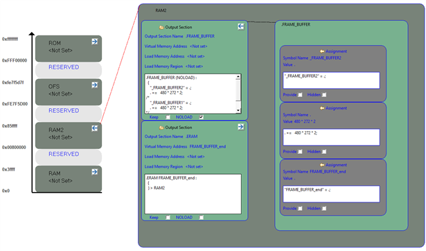
The added advantage of using the linker file is that it's documentation for the future developers. The allocated space is clearly defined and Eclipse / e2 studio have a memory visualisation display.

See the header image of this post for the graphical representation that's available.


Manage the Buffers with GCC Linker


The linker script describes the controller's memory areas and dictates what pieces of firmware go in what areas.

In e2 studio, if you create a Renesas GCC project, you'll find the script - linker_script.ld - in the src folder.

By default, a set of blocks are predefined:


MEMORY
{
RAM : ORIGIN = 0x0, LENGTH = 262144
RAM2 : ORIGIN = 0x00800000, LENGTH = 393216
ROM : ORIGIN = 0xFFF00000, LENGTH = 1048576
OFS : ORIGIN = 0xFE7F5D00, LENGTH = 128
}


(actually, RAM2 is defined as RAM2 : ORIGIN = 0x00080000, but I think that this is incorrect.)


For this exercise, let's use the 2nd block of RAM available in this controller, called On-chip expansion RAM in the datasheet extract below:

image

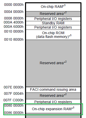
image source: annotated from Renesas RX65N data sheet


In the linker file, this memory area is named RAM2, and not used to place any objects by default. It's an unmanaged area out-of-box.

I'll be using it to fix an area for the frame buffer. Anything else placed in that memory part in later developments (E.g.: an additional frame buffer, a chunk of code, data, freely allocatable memory) will be placed after that chunk.


SECTIONS
{
// ...
  .FRAME_BUFFER (NOLOAD) : 
  {
    "_FRAME_BUFFER2" = .;  
    . +=   480 * 272 * 2;
/*
    "_FRAME_BUFFER1" = .;
    . +=   480 * 272 * 2;
*/
    "FRAME_BUFFER_end" = .;
  } > RAM2
  .ERAM FRAME_BUFFER_end : 
  {
  } > RAM2
}


The .FRAME_BUFFER section will take the first chunk of the expansion RAM. It's the first section that's told to place itself in RAM2 (> RAM2).

So it's guaranteed to be at the memory address 0x008000000.

I declared a label called _FRAME_BUFFER_2, with address . (current).

That can later be used (it becomes a variable name with known address) in our C firmware to tell the LCD library where the buffer is allocated, without hard-coding the address in the C code. I'll come back on that in the Firmware description.

Then I tell the linker to skip (fill) 480 * 272 * 2 bytes. This represents a LCD size of 480 * 272, and 2 bytes per pixel for the colour value.

It doesn't actually physically do anything with that area, not at loading and not during runtime. The area is not loaded nor initialised. But it's occupied and won't be taken by something else.


I've placed a commented out placeholder for the other buffer. My program does not use tha buffer so I didn't reserve it.

Note that there is actually not enough expansion RAM to store a second buffer with that size. Just comment out the declaration and try to build the program.

The linker will fail with a message that you are overrunning the RAM2 area. That was one of the purposes of this blog - having the linker support and guard memory management.

If you'd just hardcode the start addresses for the 2 buffers in your C program, nothing would warn you that te second chunk overruns into the reserved memory area at 0x00108000. correction - thank you Andrew J  : 0x00860000.

The datasheet says "Note 2. Reserved areas should not be accessed" but you'd find that out by the program crashing during paint commands instead of the build process flagging it.


Then I've created a label .FRAME_BUFFER_end, that's representing the first address after the memory space taken by the buffer(s).

That's used as a start point for the next section, named .ERAM by me. This section is the remainder of the expansion RAM, free to use for other purposes.


Use the Buffer in Firmware


The label _FRAME_BUFFER_2 that I created in the linker file in the previous section, automagically becomes a C external variable.

It doesn't have a type or size, but it has a known address - the adders 0x00800000 that we wanted.


Here's how we get to know the address reserved for frame buffer 2:


/* Frame buffer address of graphics 2 is the FRAME_BUFFER section top address */
extern uint32_t FRAME_BUFFER2[];
 #define FRAME_BUF_BASE_ADDR   FRAME_BUFFER2


The type of the variable isn't critical because it isn't allocated. I've used the type that's expected by the library. If the buffer is an array of consistent types, it's useful to declare it as that.

It's good for the understanding and you will not have to cast the definition to the expected type later.


    /* ==== User setting parameter ==== */
    /* ---- Graphic 2 setting ---- */
    /* Image format */
    gs_glcdc_init_cfg.input[GLCDC_FRAME_LAYER_2].p_base        = FRAME_BUF_BASE_ADDR;


The end result is that the buffer area is managed by the linker and that we don't have to hardcode buffer addresses in the C code.


For reference, here's the relevant part of the linker map output file:


.FRAME_BUFFER   0x00800000    0x3fc00
                0x00800000                _FRAME_BUFFER2 = .
                0x0083fc00                . = (. + 0x3fc00)
 *fill*         0x00800000    0x3fc00 
                0x0083fc00                FRAME_BUFFER_end = .

.ERAM


As added advantage, the location and size is documented  -  that helps when doing later maintenance to the code.

And if needed, the buffer can be moved to another location without having to adapt the code. It's good to have the linker manage what goes where.


Related blog
part 1: Create an Empty Project
part 2a: Blinky with GCC Toolchain
part 2b: Blinky with Timer and Interrupt
part 3: Port an example from Renesas toolchain to GCC
part 4a: Low Power - Sleep
part 4b: Low Power - Software Standby
4c todo: power mode 3
4d todo: power mode 4
part 5: DAC
part 6: Software SHA
part 7: Blinky with FreeRTOS
part 8: DMA
part 9: UART
part 10: Reserve LCD Frame Buffer in Expansion RAM with GCC
part 11: port emWIN to GCC and run an LCD Widget
Renesas RX65N MCU EV Kit - Review
Andrew Johnson's blog series
Renesas Envision Kit RPBRX65N Roadtest
  • Sign in to reply

Top Comments

  • Andrew J
    Andrew J over 3 years ago +3
    Interesting. I don't get why the 2nd block would overrun into the reserved area at 0x00108000. Wouldn't it overrun into the area after 0x00860000?
  • Jan Cumps
    Jan Cumps over 3 years ago in reply to Andrew J +3
    Yes - I can't count hexadecimal it seems. I looked at the wrong part of the memory map when typing it. I'll correct.
  • Jan Cumps
    Jan Cumps over 3 years ago +2
    The defect that I logged with Renesas for the wrong memory section in the GCC linker file is not going in the right direction: https://renesasrulz.com/rx/f/rx---forum/15513/ram2-section-in-gcc-linker-script…
  • Jan Cumps
    Jan Cumps over 3 years ago

    Here's how Trinamic approach fixing something in a known location. Their firmware and boot loader both expect that a structure is at a specific memory location.

    It's interesting to see this used in the real world.

    https://github.com/trinamic/TMC-EvalSystem/blob/master/main.c

    https://github.com/trinamic/TMC-EvalSystem/blob/master/hal/Landungsbruecke/freescale/MK20DN512-TMCM.ld


    In the code, they use GCC specific construct to place it in a known memory section:

    struct BootloaderConfig {
    uint32_t BLMagic;
    uint32_t drvEnableResetValue;
    };
    
    // This struct gets placed at a specific address by the linker
    struct BootloaderConfig __attribute__ ((section(".bldata"))) BLConfig;


    In the linker file, this section is placed at a known location: the begin of RAM:

    /* Specify the memory areas */
    MEMORY
    {
      m_interrupts (rx) : ORIGIN = 0x00008000, LENGTH = 0x1BC
      m_cfmprotrom (rx) : ORIGIN = 0x00008400, LENGTH = 0x10
      m_text (rx) : ORIGIN = 0x00008410, LENGTH = 512K-32K-0x410
      m_data    (rwx) : ORIGIN = 0x1FFF0000, LENGTH = 128K /* SRAM */
    }
    // ...
      /* special area for data exchange between boot loader and application
         at the beginning of the RAM*/
      .bldata (NOLOAD) :
      {
        . = ALIGN(4);
        KEEP(*(.bldata))
        . = ALIGN(4);
      } > m_data

    • Cancel
    • Vote Up +1 Vote Down
    • Sign in to reply
    • More
    • Cancel
  • Jan Cumps
    Jan Cumps over 3 years ago

    The defect that I logged with Renesas for the wrong memory section in the GCC linker file is not going in the right direction: https://renesasrulz.com/rx/f/rx---forum/15513/ram2-section-in-gcc-linker-script-starts-at-0x80000

    I raised that the project generator creates a linker file with incorrect RAM addresses and they ask me if I fixed it meanwhile image...

    • Cancel
    • Vote Up +2 Vote Down
    • Sign in to reply
    • More
    • Cancel
  • Jan Cumps
    Jan Cumps over 3 years ago

    What I didn't tell:

    If you're just interested in getting a variable or buffer into the expansion RAM, it would suffice to just create a section n the linker file, then  use:


    uuint32 __attribute__((section (".FRAME_BUFFER"))) frameBuffer[size];


    The thing with a big buffer like the LCD driver's frame buffer - especially in a microcontroller where there aren't many big chunks of memory available - is that it's hard to get 232000 bytes available in a continuous block available if you don't manage it.

    That's why in this case putting it in a known available block makes sense. The linker can have fun allocating room for te small variables. That's not hard, even in a broken memory chunk.


    What I didn't tell part 2:

    I would not use my method to reserve the memory addresses for registers and memory mapped devices.

    In that case, I'd just not make those memory chunks available in the loader script, and use header files - like the majority of HAL layers and microcontroller frameworks do for this type of memory areas.


    (

    also the Renesas tool chains do that. The red areas below are made unavailable to the linker, and the header files generate all the register addresses and structures:

    image

    )

    • Cancel
    • Vote Up +1 Vote Down
    • Sign in to reply
    • More
    • Cancel
  • Jan Cumps
    Jan Cumps over 3 years ago in reply to Andrew J

    Yes image - I can't count hexadecimal it seems. I looked at the wrong part of the memory map when typing it. I'll correct.

    • Cancel
    • Vote Up +3 Vote Down
    • Sign in to reply
    • More
    • Cancel
  • Andrew J
    Andrew J over 3 years ago

    Interesting.  I don't get why the 2nd block would overrun into the reserved area at 0x00108000.  Wouldn't it overrun into the area after 0x00860000?

    • Cancel
    • Vote Up +3 Vote Down
    • Sign in to reply
    • More
    • Cancel
element14 Community

element14 is the first online community specifically for engineers. Connect with your peers and get expert answers to your questions.

  • Members
  • Learn
  • Technologies
  • Challenges & Projects
  • Products
  • Store
  • About Us
  • Feedback & Support
  • FAQs
  • Terms of Use
  • Privacy Policy
  • Legal and Copyright Notices
  • Sitemap
  • Cookies

An Avnet Company © 2023 Premier Farnell Limited. All Rights Reserved.

Premier Farnell Ltd, registered in England and Wales (no 00876412), registered office: Farnell House, Forge Lane, Leeds LS12 2NE.

ICP 备案号 10220084.

Follow element14

  • X
  • Facebook
  • linkedin
  • YouTube