Today, 06:56 AM Today, 06:56 AM |
Hello,
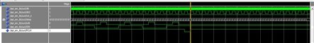
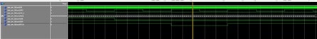
please , i want to program AD75019 , an analogue Cross point Switch from analogue devices 16x16, with FPGA, ad75019 have a serial interface, i'have to shift 256 bit into 256 bit shift register , once the register is full i apply a PCLK pulse to to transfer the register to latch (like it's mentionned in the datasheet) my problem is, that i can'T close or open any switch 
please , anyone could help, thanks in Advance
this my configuration:
VDD:11V
VCC:5V
VSS: 0V
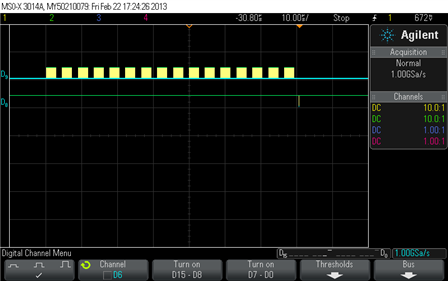
SCLK: 1MHZ
this how i did the spi interface : a shift register of 256 bit with a state machine for controlling PCLK signal:
-- spi_SM.vhd
library ieee;
use ieee.std_logic_1164.all;
use ieee.std_logic_arith.all;
use ieee.std_logic_signed.all;
use ieee.std_logic_arith.all;
entity spi_SM is
generic(N:integer :=256; C:integer :=9; D:integer :=4 );
-- generic(C:integer :=9);
port(
clk :in std_logic;
rst_n:in std_logic;
data: in std_logic_vector (N-1 downto 0);
SCLK: inout std_logic; --inout pour qu'il peut etre lu en process
SIN  ut std_logic;
PCLK: out std_logic
);
end spi_SM;
architecture rtl of spi_SM is
type States is (ACTIF, UPDATE, IDLE);
signal state : States := ACTIF;
signal EndSend : std_logic_vector(8 downto 0);
signal t_rst_cnt_n : std_logic ;
--Diviseur (pour generer la frequence d'horloge du port SPI(20Khz-5Mhz))
component diviseur
generic ( N : integer := 4 );
port(
clk : in std_logic ;
rst_n : in std_logic ;
clk_out : out std_logic
);
end component;
--Compteurnbit
component Compteurnbit
generic ( N : integer := 16 );
port(
clk : in std_logic ;
rst_cnt_n : in std_logic ;
OutCount : inout std_logic_vector(N-1 downto 0)
);
end component;
--Sregister
component Sregister
generic ( N : integer := 256 );
port(
clk : in std_logic;
rst_n : in std_logic;
S :in std_logic_vector (N-1 downto 0);-- durée de train d'impulsion
Q : out std_logic
);
end component;
begin
U0_diviseur : diviseur generic map(D) port map(clk, rst_n, SCLK); ---definir frequence de SPI (clk de base=20 Mhz)
U0_Sregister : Sregister generic map(N) port map(SCLK,rst_n,data,SIN);
U0_Compteurnbit : Compteurnbit generic map(C) port map(SCLK,t_rst_cnt_n,EndSend);-- counting 256 pulse to set EndSend
send : process (SCLK,EndSend)
begin
if (rst_n='0') then
t_rst_cnt_n<='0';
else
case state is
when
actif=>
if (unsigned(EndSend) = 256) then -- opertation arithmetique donc convertit std_logic_vector en unsigned
PCLK<='0';--0
t_rst_cnt_n<='0';
state<= UPDATE;
else
t_rst_cnt_n<='1';
PCLK<='1';
state<= ACTIF;
end if;
when UPDATE=>
PCLK<='1';--0
-- state<= actif ;
state<= IDLE;
when IDLE=>
PCLK<='1';
state<= IDLE;
end case;
end if;
end process;
end;