element14 Community
element14 Community
    Register Log In
  • Site
  • Search
  • Log In Register
  • About Us
  • Community Hub
    Community Hub
    • What's New on element14
    • Feedback and Support
    • Benefits of Membership
    • Personal Blogs
    • Members Area
    • Achievement Levels
  • Learn
    Learn
    • Ask an Expert
    • eBooks
    • element14 presents
    • Learning Center
    • Tech Spotlight
    • STEM Academy
    • Webinars, Training and Events
    • Learning Groups
  • Technologies
    Technologies
    • 3D Printing
    • FPGA
    • Industrial Automation
    • Internet of Things
    • Power & Energy
    • Sensors
    • Technology Groups
  • Challenges & Projects
    Challenges & Projects
    • Design Challenges
    • element14 presents Projects
    • Project14
    • Arduino Projects
    • Raspberry Pi Projects
    • Project Groups
  • Products
    Products
    • Arduino
    • Avnet Boards Community
    • Dev Tools
    • Manufacturers
    • Multicomp Pro
    • Product Groups
    • Raspberry Pi
    • RoadTests & Reviews
  • Store
    Store
    • Visit Your Store
    • Choose another store...
      • Europe
      •  Austria (German)
      •  Belgium (Dutch, French)
      •  Bulgaria (Bulgarian)
      •  Czech Republic (Czech)
      •  Denmark (Danish)
      •  Estonia (Estonian)
      •  Finland (Finnish)
      •  France (French)
      •  Germany (German)
      •  Hungary (Hungarian)
      •  Ireland
      •  Israel
      •  Italy (Italian)
      •  Latvia (Latvian)
      •  
      •  Lithuania (Lithuanian)
      •  Netherlands (Dutch)
      •  Norway (Norwegian)
      •  Poland (Polish)
      •  Portugal (Portuguese)
      •  Romania (Romanian)
      •  Russia (Russian)
      •  Slovakia (Slovak)
      •  Slovenia (Slovenian)
      •  Spain (Spanish)
      •  Sweden (Swedish)
      •  Switzerland(German, French)
      •  Turkey (Turkish)
      •  United Kingdom
      • Asia Pacific
      •  Australia
      •  China
      •  Hong Kong
      •  India
      •  Korea (Korean)
      •  Malaysia
      •  New Zealand
      •  Philippines
      •  Singapore
      •  Taiwan
      •  Thailand (Thai)
      • Americas
      •  Brazil (Portuguese)
      •  Canada
      •  Mexico (Spanish)
      •  United States
      Can't find the country/region you're looking for? Visit our export site or find a local distributor.
  • Translate
  • Profile
  • Settings
Experts, Learning and Guidance
  • Technologies
  • More
Experts, Learning and Guidance
Ask an Expert Forum Need Help Interpreting Schematic and circuit design for L4971 DC to DC Switching Regulator
  • Blog
  • Forum
  • Documents
  • Leaderboard
  • Files
  • Members
  • Mentions
  • Sub-Groups
  • Tags
  • More
  • Cancel
  • New
Join Experts, Learning and Guidance to participate - click to join for free!
Actions
  • Share
  • More
  • Cancel
Forum Thread Details
  • State Suggested Answer
  • Replies 8 replies
  • Answers 4 answers
  • Subscribers 290 subscribers
  • Views 1677 views
  • Users 0 members are here
  • l4971_switching_regulator
Related
See a helpful answer?

Be sure to click 'more' and select 'suggest as answer'!

If you're the thread creator, be sure to click 'more' then 'Verify as Answer'!

Need Help Interpreting Schematic and circuit design for L4971 DC to DC Switching Regulator

jw0752
jw0752 over 5 years ago

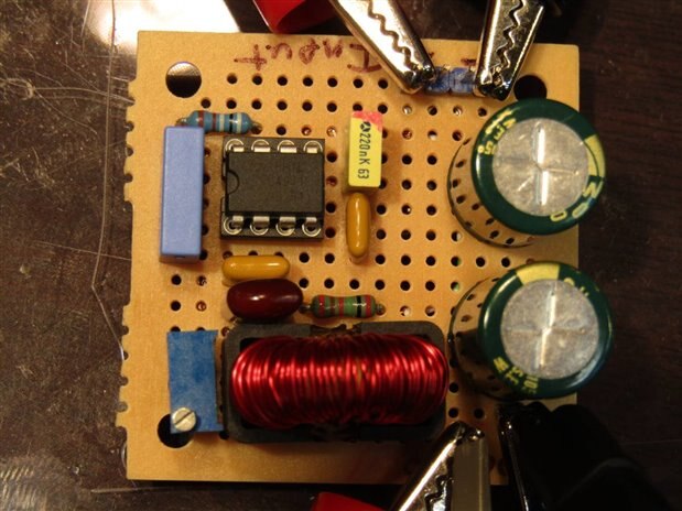
I have recently been experimenting with the L4971 DC to DC Buck Switching Regulator IC.


http://www.farnell.com/datasheets/1689801.pdf?_ga=2.69477264.1687415617.1589140235-732132915.1579132131://


I discovered this IC chip when a number of them were salvaged from a power supply board. My question involves the interpretation of the unusual way that the schematic for a test circuit is drawn in the manufacturer's data sheet. (see above link) and the reason for this peculiar design feature.


Here is the schematic as drawn on page one of the L4971 data sheet:


image


As you can see the negative rail enters the schematic at the bottom left as is conventional and carries across the page to the bottom right. There are three components that connect directly to the negative rail and then a secondary negative rail is drawn from a connection at the bottom right and back towards the left onto which the ground connections from the chip itself as well as a couple of other components are attached.


The Data Sheet also provides a template for a circuit board:


image


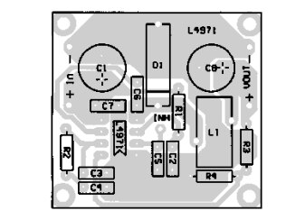
The board does reflect the drawing of the schematic as it has two large negative rail pads on the upper and lower sections of the circuit board with a narrower, though still substantial, trace between them.


How does this particular design help the function of this switching regulator and why is it important enough to require the unusual reflection in the drawing of the schematic?


The Data sheet doesn't seem to cover this intricacy of the design. Any insights that anyone might have will be appreciated.


John

  • Sign in to reply
  • Cancel

Top Replies

  • jw0752
    jw0752 over 5 years ago +7 suggested
    As I mentioned I have built the circuit on a piece of perf-board this evening and here is what it looks like: The performance, compared to the bread board of last night, was excellent. Last night I was…
  • shabaz
    shabaz over 5 years ago +6 suggested
    Hi John, Usually that style schematic is done just to provide a signal to the PCB designer (since that person will be different to the electronics design engineer who will have drawn the schematic) to…
  • Andrew J
    Andrew J over 5 years ago in reply to jw0752 +4 suggested
    Hi John, pin7 is for frequency compensation at the error amplifier to try and stabilise the response during changes of external influences (input voltage, load changes etc.) good explanation here - the…
  • shabaz
    0 shabaz over 5 years ago

    Hi John,


    Usually that style schematic is done just to provide a signal to the PCB designer (since that person will be different to the electronics design engineer who will have drawn the schematic) to consult with the design engineer, i.e. like a written note on the schematic. In this case, it is (I think) trying to show the high current path, being the lower drawn rail, and the lower current path preferred point of physical connection, being the rail above it. I think the important thing there is that the IC ground and the circuitry on the compensation pin (pin 7) are together at one point, and taken as close as possible from the output end of the rail, because any regulation (the feedback pin is internal to this IC) will be connected to the output end too. In other words, the error amplifier related circuitry visible in the block diagram in the datasheet is out of the high current path. So, there won't be voltage drop associated noise in this feedback portion of the chip, were the pins separated, or connected near the input end if the lower rail was thin and had resistance. The layout looks single-sided according to that PCB template so probably it was important to highlight it in this way. It might look different for a more recent IC datasheet with a 2-layer implementation with a dedicated ground plane, i.e. it might become less critical (just guessing).

    • Cancel
    • Vote Up +6 Vote Down
    • Sign in to reply
    • Verify Answer
    • Reject Answer
    • Cancel
  • jw0752
    0 jw0752 over 5 years ago in reply to shabaz

    Hi Shabaz,


    Thank you for taking the time to give me these excellent insights into what is going on. It all makes better sense in view of your explanation. I put the circuit on a bread board last night but I was not happy with the regulation nor the ripple. I am going to build it again tonight only this time on a piece of perf-board and use the layout provided on the sample board. I want to see if I can improve the regulation and quality of the output. The ICs were being used on a power supply for an expensive Dental X-Ray system so I have a feeling that any quality problems relate more to my bread board set up than to the engineering of the chip or the circuit. The board that I took the parts from used the same data sheet circuit for their design right down to the precise values of the resistors so if I can figure out how to put SMD parts on a perf-board I will be all set.


    John

    • Cancel
    • Vote Up +3 Vote Down
    • Sign in to reply
    • Verify Answer
    • Reject Answer
    • Cancel
  • jw0752
    0 jw0752 over 5 years ago

    As I mentioned I have built the circuit on a piece of perf-board this evening and here is what it looks like:


    imageimage


    The performance, compared to the bread board of last night, was excellent. Last night I was very disappointed with the ability of the circuit to regulate as the load was increased. Tonight however the perf-board version was very stable. I began with the voltage set at 10.01 Volts and no load. When I got to 750 mA of load the voltage had only dropped by 30 millivolts. With the input voltage at 20 volts and the output set to 10 volts and 750 mA load I found that the efficiency was 90%.


    I have installed a resistive trimmer so that I can adjust the voltage output (Blue Trimmer in lower left corner). The trimmer gives me the ability to adjust the output from 3.3 volts up to about 21 volts as long as the input voltage is 400 mV above the output voltage. I was really surprised to find that there is only 0.4 volts dropout.


    I have one more question if anyone can help. The schematic doesn't show capacitor C3 but the board layout shows C3 between pin 7 of the L4971 and Ground. Pin 7 is used for external adjustment of the frequency of the switch. My board is currently running at about 100 kHz. What would be the purpose of C3 if they have left it off the schematic but included a place for it on the circuit board template?


    Thanks John

    • Cancel
    • Vote Up +7 Vote Down
    • Sign in to reply
    • Verify Answer
    • Reject Answer
    • Cancel
  • Andrew J
    0 Andrew J over 5 years ago in reply to jw0752

    Hi John,


    pin7 is for frequency compensation at the error amplifier to try and stabilise the response during changes of external influences (input voltage, load changes etc.)


    good explanation here - the set up on the board is described towards the end.  It’s to help deal with noise on the output from just having the RC connection.  https://www.digikey.co.uk/en/articles/designing-compensator-networks-to-improve-switching-regulator-frequency-response

    • Cancel
    • Vote Up +4 Vote Down
    • Sign in to reply
    • Verify Answer
    • Reject Answer
    • Cancel
  • jw0752
    0 jw0752 over 5 years ago in reply to Andrew J

    Hi Andrew,


    Thank you very much for finding and linking the article on compensator networks. It will help me understand what is going on.


    John

    • Cancel
    • Vote Up +3 Vote Down
    • Sign in to reply
    • Verify Answer
    • Cancel
  • shabaz
    0 shabaz over 5 years ago in reply to jw0752

    Hi John,


    Great compact prototyping! Nice to see the Radio Shack board too.

    • Cancel
    • Vote Up +3 Vote Down
    • Sign in to reply
    • Verify Answer
    • Cancel
  • genebren
    0 genebren over 5 years ago in reply to jw0752

    Nice work John.  The cleanliness of your builds always impresses me, as does your tenacity to stick with a problem and look for a better solution.  You help us all dig a little deeper.

    • Cancel
    • Vote Up +2 Vote Down
    • Sign in to reply
    • Verify Answer
    • Cancel
  • jw0752
    0 jw0752 over 5 years ago in reply to genebren

    Thanks, Gene and Shabaz,

    I really appreciate your help and support.


    John

    • Cancel
    • Vote Up +1 Vote Down
    • Sign in to reply
    • Verify Answer
    • Cancel
element14 Community

element14 is the first online community specifically for engineers. Connect with your peers and get expert answers to your questions.

  • Members
  • Learn
  • Technologies
  • Challenges & Projects
  • Products
  • Store
  • About Us
  • Feedback & Support
  • FAQs
  • Terms of Use
  • Privacy Policy
  • Legal and Copyright Notices
  • Sitemap
  • Cookies

An Avnet Company © 2025 Premier Farnell Limited. All Rights Reserved.

Premier Farnell Ltd, registered in England and Wales (no 00876412), registered office: Farnell House, Forge Lane, Leeds LS12 2NE.

ICP 备案号 10220084.

Follow element14

  • X
  • Facebook
  • linkedin
  • YouTube