element14 Community
element14 Community
    Register Log In
  • Site
  • Search
  • Log In Register
  • Community Hub
    Community Hub
    • What's New on element14
    • Feedback and Support
    • Benefits of Membership
    • Personal Blogs
    • Members Area
    • Achievement Levels
  • Learn
    Learn
    • Ask an Expert
    • eBooks
    • element14 presents
    • Learning Center
    • Tech Spotlight
    • STEM Academy
    • Webinars, Training and Events
    • Learning Groups
  • Technologies
    Technologies
    • 3D Printing
    • FPGA
    • Industrial Automation
    • Internet of Things
    • Power & Energy
    • Sensors
    • Technology Groups
  • Challenges & Projects
    Challenges & Projects
    • Design Challenges
    • element14 presents Projects
    • Project14
    • Arduino Projects
    • Raspberry Pi Projects
    • Project Groups
  • Products
    Products
    • Arduino
    • Avnet & Tria Boards Community
    • Dev Tools
    • Manufacturers
    • Multicomp Pro
    • Product Groups
    • Raspberry Pi
    • RoadTests & Reviews
  • About Us
    About the element14 Community
  • Store
    Store
    • Visit Your Store
    • Choose another store...
      • Europe
      •  Austria (German)
      •  Belgium (Dutch, French)
      •  Bulgaria (Bulgarian)
      •  Czech Republic (Czech)
      •  Denmark (Danish)
      •  Estonia (Estonian)
      •  Finland (Finnish)
      •  France (French)
      •  Germany (German)
      •  Hungary (Hungarian)
      •  Ireland
      •  Israel
      •  Italy (Italian)
      •  Latvia (Latvian)
      •  
      •  Lithuania (Lithuanian)
      •  Netherlands (Dutch)
      •  Norway (Norwegian)
      •  Poland (Polish)
      •  Portugal (Portuguese)
      •  Romania (Romanian)
      •  Russia (Russian)
      •  Slovakia (Slovak)
      •  Slovenia (Slovenian)
      •  Spain (Spanish)
      •  Sweden (Swedish)
      •  Switzerland(German, French)
      •  Turkey (Turkish)
      •  United Kingdom
      • Asia Pacific
      •  Australia
      •  China
      •  Hong Kong
      •  India
      •  Japan
      •  Korea (Korean)
      •  Malaysia
      •  New Zealand
      •  Philippines
      •  Singapore
      •  Taiwan
      •  Thailand (Thai)
      •  Vietnam
      • Americas
      •  Brazil (Portuguese)
      •  Canada
      •  Mexico (Spanish)
      •  United States
      Can't find the country/region you're looking for? Visit our export site or find a local distributor.
  • Translate
  • Profile
  • Settings
Experts, Learning and Guidance
  • Technologies
  • More
Experts, Learning and Guidance
Ask an Expert Forum Trying to understand serial to parallel circuit
  • Blog
  • Forum
  • Documents
  • Leaderboard
  • Files
  • Members
  • Mentions
  • Sub-Groups
  • Tags
  • More
  • Cancel
  • New
Join Experts, Learning and Guidance to participate - click to join for free!
Actions
  • Share
  • More
  • Cancel
Forum Thread Details
  • State Not Answered
  • Replies 32 replies
  • Subscribers 330 subscribers
  • Views 10355 views
  • Users 0 members are here
Related
See a helpful answer?

Be sure to click 'more' and select 'suggest as answer'!

If you're the thread creator, be sure to click 'more' then 'Verify as Answer'!

Trying to understand serial to parallel circuit

opalko
opalko over 4 years ago

Hi again folks (after some time away!),
When I was a teen, I had an Atari 800 computer/ The Atari did not have a parallel port interface.  All they had were the joystick ports, which were serial.  A clever company came up with a serial->parallel port interface.  Me, not knowing much about electronics, could not figure out how they did this.  (PS -I still don't know much about electronics!!!).

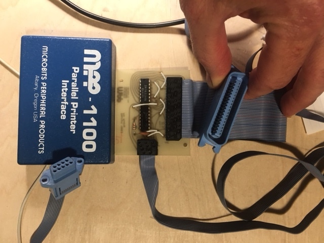
Flash forward 40 years and this past week I decided to take apart the serial->parallel interface and reverse engineer this thing! I took apart and there are 2 chips - a 74LS14, and a 74LS164, a resistor and a capacitor. Next step was to draw the schematic, which I did with pencil and paper. This became messy, so I resorted to learning to use KiCad, and came up with the attached drawing. (see attachments)

I get what makes this work is the 74LS164 8 bit parallel-out serial shift register. I still don't really understand how it works though.  As I understand it, the data on this register may be read out in parallel (from all flip-flops) at once.
So some questions!

0) Can someone explain how this whole interface works!?

1) How is the data being read on the printer side?  Is the printer polling every data pin on the parallel port at once regardless of how many are actually being used?

2) Since there are really only 2 address data pins (3 & 5) being used here, it doesn't seem a vast improvement over serial?  But I guess because the Atari only has pins 1-4 for I/O and 1 of those sends the data to the 74LS164?

Thanks for any help understanding this.
Robert Opalko

PS There doesn't seem to be nearly as many members on this forum as there was in the past... Where did everyone go?

image
image
  • Sign in to reply
  • Cancel

Top Replies

  • phoenixcomm
    phoenixcomm over 4 years ago in reply to opalko +4
    try this link: computer.howstuffworks.com/parallel-port1.htm this says that IBM did it but in fact, It was Wang labs. and en.wikipedia.org/.../Centronics
  • phoenixcomm
    phoenixcomm over 4 years ago +4
  • dougw
    dougw over 4 years ago +3
    I don't get it either. A Centronics printer needs 8 data bits and some handshaking to work - this doesn't even have enough pins connected. On a Centronics connector all pins from 19-30 and 33 are ground…
  • opalko
    0 opalko over 4 years ago in reply to beacon_dave

    This is why I like this forum above others; always great help and folks are encouraging rather than saying what a dummy you are (even when I make dumb mistakes like I did here not finishing mapping everything!)

    • Cancel
    • Vote Up +1 Vote Down
    • Sign in to reply
    • Verify Answer
    • Cancel
  • phoenixcomm
    0 phoenixcomm over 4 years ago

    image

    • Cancel
    • Vote Up +4 Vote Down
    • Sign in to reply
    • Verify Answer
    • Cancel
  • opalko
    0 opalko over 4 years ago in reply to beacon_dave
    beacon_dave said:
    Looks like your schematic is missing an inverter gate as well.

    Wait, I am counting 8 traces going to the 74LS14

    pin 1 (inverter 1A) -> DB9 pin 2
    pin 2 (inverter 1Y) -> 74LS164 pin 8 (CLK)
    pin 3 (inverter 2A) -> DB9 pin 4
    pin 4 (inverter 2Y) -> Centronics pin 1
    pin 10 (inverter 5A) -> Centronics pin 13
    pin 11 (inverter 5Y) -> DB9 pin 6 (joystick port trigger input)
    These 6 are on my schematic, and then there are
    pin 14 (Vcc)
    pin 7 (GND) - these 2 I didn't know how to show as KiCad only gave me inverters for the 74LS14, no options for GND or Vcc pins..

    Is there another inverter? I did get the labeling wrong for inverter 5A/5Y on schematic, it says 5/6 when it should be pins 10/11.

    beacon_dave said:
    Looks like Out 5 heads to the 9-pin connector.

    I think this is correct though? Thinking

    • Cancel
    • Vote Up 0 Vote Down
    • Sign in to reply
    • Verify Answer
    • Cancel
  • opalko
    0 opalko over 4 years ago in reply to beacon_dave
    beacon_dave said:
    The 8 data lines are there and mapping to the correct printer pins. 

    Thank you writing out this mapping! Wow, I really screwed up the mapping the first time I did this (it was rather late). I was getting the numbering mixed up thinking the lines were odd numbers 1-17 in the row closest to the board edge, then 2-18 in the next row, then 19- , and finally 20-36 in the last row. No wonder I couldn't get it mapped correctly. Now that I see it goes 1-2-3-4 and follows the ribbons "down", and then starts over at 5-6-7-8 etc.

    • Cancel
    • Vote Up 0 Vote Down
    • Sign in to reply
    • Verify Answer
    • Cancel
  • beacon_dave
    0 beacon_dave over 4 years ago in reply to opalko

    Ok, mislabeled inverter then. Three of the six are used.

    • Cancel
    • Vote Up +1 Vote Down
    • Sign in to reply
    • Verify Answer
    • Cancel
  • beacon_dave
    0 beacon_dave over 4 years ago in reply to opalko

    Connectors can be a little bit tricky with their numbering schemes at times. Ribbons are a bit more predictable, although here it looks like you have a 9-way ribbon terminated in a 10-way PCB connector so need to watch out for things like that.

    It looks like you should have a more sensible looking schematic now. 

    • Cancel
    • Vote Up +1 Vote Down
    • Sign in to reply
    • Verify Answer
    • Cancel
  • beacon_dave
    0 beacon_dave over 4 years ago
    opalko said:
    0) Can someone explain how this whole interface works!?

    Clocked serial data comes in via the 9-pin Atari interface into the shift register. After input 8 clocks the shift register holds 1 byte of data and the printer is strobed to tell it to look at the 8-bit data in parallel. There are some additional control lines for the computer to reset the printer and for the printer to tell the computer that it is selected and that it is ready to receive more data or not. The cycle repeats, 8bits clocked in, 1 byte clocked out. Some signals are active high and some active low, so logic inverters are used to flip the signal as required.

    The 'magic' pretty much happens in the shift register, so take a look at Karen's video on shift registers (serial in parallel out mode). 

    • Cancel
    • Vote Up +3 Vote Down
    • Sign in to reply
    • Verify Answer
    • Cancel
  • beacon_dave
    0 beacon_dave over 4 years ago
    opalko said:
    1) How is the data being read on the printer side?  Is the printer polling every data pin on the parallel port at once regardless of how many are actually being used?

    Once the shift register has 8 bits clocked into it, the data bus has 8 bits set. The printer is strobed by the computer to tell it that the data is now ready to be read. All 8 data pins are being used, they hold a byte value in binary with high and low voltages representing 1's and 0's. If the printer is in plain text mode you will find that the data is ASCII values for each character being printed. There are some 'magic values' that tell the printer to change its mode rather than printing the character. You need to refer to the printer's manual to see what those values are. Some are pretty standard, others are printer specific.  

    • Cancel
    • Vote Up +3 Vote Down
    • Sign in to reply
    • Verify Answer
    • Cancel
  • beacon_dave
    0 beacon_dave over 4 years ago
    opalko said:
    2) Since there are really only 2 address data pins (3 & 5) being used here, it doesn't seem a vast improvement over serial?  But I guess because the Atari only has pins 1-4 for I/O and 1 of those sends the data to the 74LS164?

    I think we can probably skip over this one due to the errors found in the original schematic. Probably less of a performance issue and more of a compatibility issue as the Atari didn't have a Centronics parallel interface and a lot of printers didn't have a serial interface, so a convertor was required just to get the two to talk. Also with home printers, speed was often limited by the speed of the printer mechanics. Some had larger memory buffer options that allowed you to dump the data into the printer and leave it to do its own thing whilst you used the computer for something else, but that bumped up the cost. Some commercial line printers did however go really fast. 

    (...which reminds me a531016 how about a tear down of an old line printer for an episode of The Electronics Inside ? )

    • Cancel
    • Vote Up +3 Vote Down
    • Sign in to reply
    • Verify Answer
    • Cancel
  • phoenixcomm
    0 phoenixcomm over 4 years ago in reply to opalko

    Re: you have a uni-direction printer cable. When the printer is busy it sets 'BUSY' active and the computer stops sending data. conversely, when the BUSY is NOT ACTIVE the computer will send data. The same is true for the ON-LINE Signal the must be active for anything to work.  

    • Cancel
    • Vote Up +3 Vote Down
    • Sign in to reply
    • Verify Answer
    • Cancel
<>
element14 Community

element14 is the first online community specifically for engineers. Connect with your peers and get expert answers to your questions.

  • Members
  • Learn
  • Technologies
  • Challenges & Projects
  • Products
  • Store
  • About Us
  • Feedback & Support
  • FAQs
  • Terms of Use
  • Privacy Policy
  • Legal and Copyright Notices
  • Sitemap
  • Cookies

An Avnet Company © 2026 Premier Farnell Limited. All Rights Reserved.

Premier Farnell Ltd, registered in England and Wales (no 00876412), registered office: Farnell House, Forge Lane, Leeds LS12 2NE.

ICP 备案号 10220084.

Follow element14

  • X
  • Facebook
  • linkedin
  • YouTube