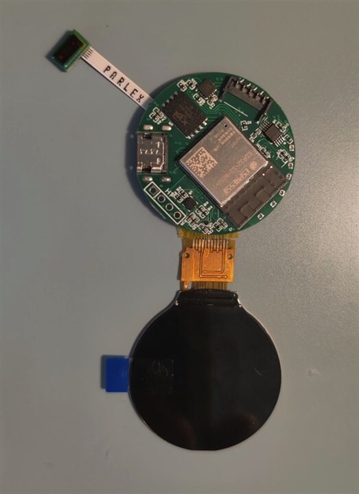
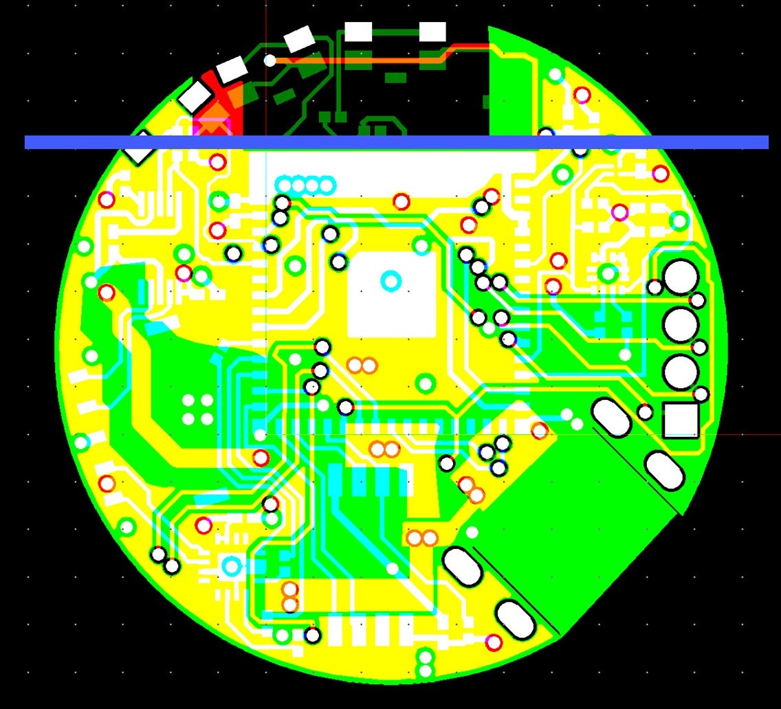
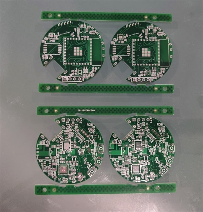
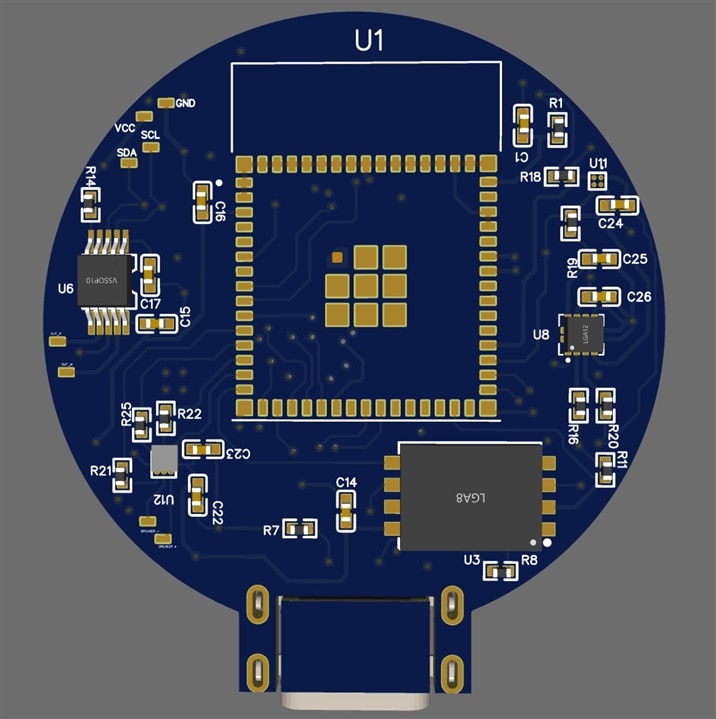
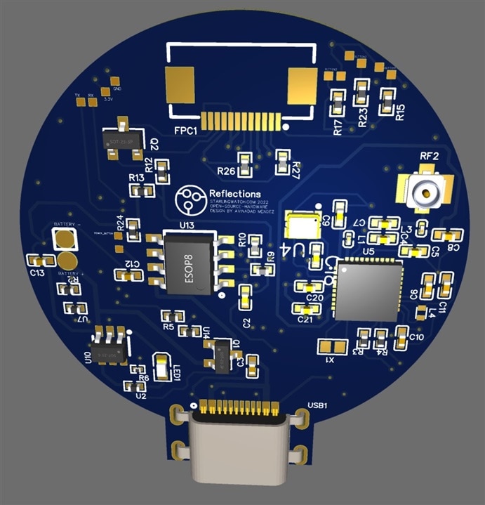
Hi 14-ers, this is my first post to the forums. I hope it's not too strange of a question. I am excited to be working on a new open-source platform (hardware and software) for making mobile storytelling experiences. (https://github.com/frankcohen/ReflectionsOS). I hired a freelance PCB designer to take my breadboard and create the schematic and layout. I will be taking the design to a board assembly company to build prototypes - along the path to manufacturing. I am new to the PCB designer community. Is it acceptable practice to ask other PCB designers here to review the schematic and layout? Is Element14 forums the right place? Should I hire someone to be a reviewer? I'm thinking the more eyes on it the better it will be. -Frank
Show less


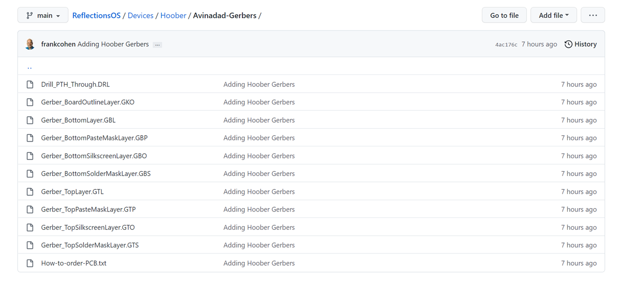
 I will be publishing the EasyEDA project and Gerber files this week. -Frank