


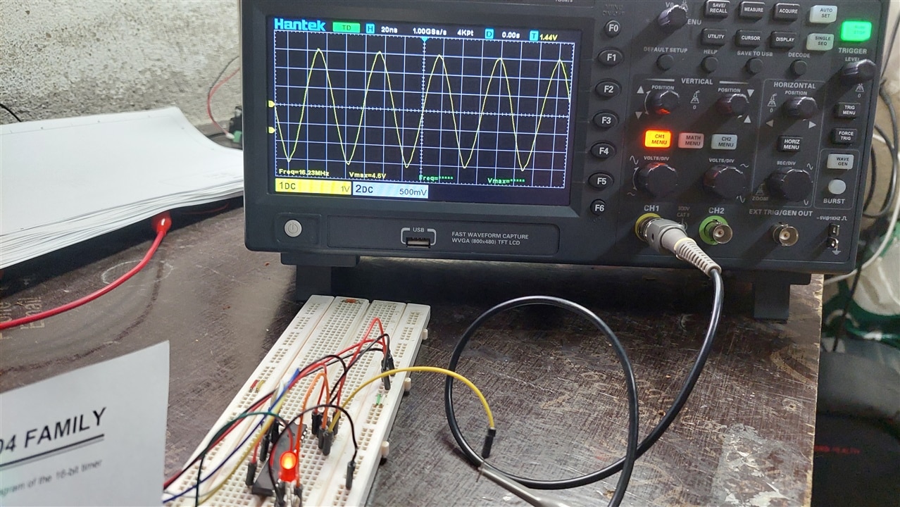
I hello. I'm trying , config the timer1 from pic24fj128ga, but without success. anyone there can´try to help me, please.
I already have config the configuration bit. I have the REFO with 16MHz.
// CONFIG4
#pragma config DSWDTPS = DSWDTPS1F      // Deep Sleep Watchdog Timer Postscale Select bits (1:68719476736 (25.7 Days))
#pragma config DSWDTOSC = LPRC          // DSWDT Reference Clock Select (DSWDT uses LPRC as reference clock)
#pragma config DSBOREN = OFF            // Deep Sleep BOR Enable bit (DSBOR Disabled)
#pragma config DSWDTEN = OFF            // Deep Sleep Watchdog Timer Enable (DSWDT Disabled)
#pragma config DSSWEN = OFF             // DSEN Bit Enable (Deep Sleep operation is always disabled)
#pragma config PLLDIV = PLL4X           // USB 96 MHz PLL Prescaler Select bits (4x PLL selected)
#pragma config I2C1SEL = DISABLE        // Alternate I2C1 enable bit (I2C1 uses SCL1 and SDA1 pins)
#pragma config IOL1WAY = OFF            // PPS IOLOCK Set Only Once Enable bit (The IOLOCK bit can be set and cleared using the unlock sequence)

// CONFIG3
#pragma config WPFP = WPFP0             // Write Protection Flash Page Segment Boundary (Page 0 (0x00))
#pragma config SOSCSEL = OFF            // SOSC Selection bits (Digital (SCLKI) mode)
#pragma config WDTWIN = PS25_0          // Window Mode Watchdog Timer Window Width Select (Watch Dog Timer Window Width is 25 percent)
#pragma config PLLSS = PLL_FRC          // PLL Secondary Selection Configuration bit (PLL is fed by the on-chip Fast RC (FRC) oscillator)
#pragma config BOREN = OFF              // Brown-out Reset Enable (Brown-out Reset Disabled)
#pragma config WPDIS = WPDIS            // Segment Write Protection Disable (Disabled)
#pragma config WPCFG = WPCFGDIS         // Write Protect Configuration Page Select (Disabled)
#pragma config WPEND = WPSTARTMEM       // Segment Write Protection End Page Select (Write Protect from page 0 to WPFP)

// CONFIG2
#pragma config POSCMD = NONE            // Primary Oscillator Select (Primary Oscillator Disabled)
#pragma config WDTCLK = LPRC            // WDT Clock Source Select bits (WDT uses LPRC)
#pragma config OSCIOFCN = OFF           // OSCO Pin Configuration (OSCO/CLKO/RA3 functions as CLKO (FOSC/2))
#pragma config FCKSM = CSDCMD           // Clock Switching and Fail-Safe Clock Monitor Configuration bits (Clock switching and Fail-Safe Clock Monitor are disabled)
#pragma config FNOSC = FRCPLL           // Initial Oscillator Select (Fast RC Oscillator with PLL module (FRCPLL))
#pragma config ALTCMPI = CxINC_RB       // Alternate Comparator Input bit (C1INC is on RB13, C2INC is on RB9 and C3INC is on RA0)
#pragma config WDTCMX = WDTCLK          // WDT Clock Source Select bits (WDT clock source is determined by the WDTCLK Configuration bits)
#pragma config IESO = OFF               // Internal External Switchover (Disabled)

// CONFIG1
#pragma config WDTPS = PS32768          // Watchdog Timer Postscaler Select (1:32,768)
#pragma config FWPSA = PR128            // WDT Prescaler Ratio Select (1:128)
#pragma config WINDIS = OFF             // Windowed WDT Disable (Standard Watchdog Timer)
#pragma config FWDTEN = OFF             // Watchdog Timer Enable (WDT disabled in hardware; SWDTEN bit disabled)
#pragma config ICS = PGx1               // Emulator Pin Placement Select bits (Emulator functions are shared with PGEC1/PGED1)
#pragma config LPCFG = OFF              // Low power regulator control (Disabled - regardless of RETEN)
#pragma config GWRP = OFF               // General Segment Write Protect (Write to program memory allowed)
#pragma config GCP = OFF                // General Segment Code Protect (Code protection is disabled)
#pragma config JTAGEN = ON              // JTAG Port Enable (Enabled)

// #pragma config statements should precede project file includes.
// Use project enums instead of #define for ON and OFF.

#include <xc.h>
the timer.c its config:
#include <stdio.h>
#include <stdlib.h>
#include <stdbool.h>
#include <xc.h>

#include "Timer1.h"

uint16_t timer_delay_ms_UI16 = 0;
uint16_t timer_heartbeat_ms_UI16 = 250;

/* Example code for Timer1 ISR*/
void __attribute__((__interrupt__, __no_auto_psv__)) _T1Interrupt(void)
{
    /* Interrupt Service Routine code goes here */
//    if(timer_delay_ms_UI16>0)
//    {
//        timer_delay_ms_UI16--;
//    }
//    if(timer_heartbeat_ms_UI16>0)
//    {
//        timer_heartbeat_ms_UI16--;
//    }

    timer_delay_ms_UI16=1;
    IFS0bits.T1IF = 0; //Reset Timer1 interrupt flag and Return from ISR

}

void my_delay_ms(uint16_t time_to_my_delay_UI16)
{
    timer_delay_ms_UI16 = time_to_my_delay_UI16;
    while(timer_delay_ms_UI16>0);
}

 void Init_TIMER(void)
{
    /* The following code example will enable Timer1 interrupts, load the Timer1
    Period register and start Timer1.
     *
    When a Timer1 period match interrupt occurs, the interrupt service
    routine must clear the Timer1 interrupt status flag in software.
    */
    TMR1 = 0x00;//Clear contents of the timer register
    T1CON = 0x00;//Stops the Timer1 and reset control reg.
    TMR1 = 0x00;//Clear contents of the timer register

    //Set Timer 1 period register
    //Fosc = 32 KHz
    //Tosc= 1/32k=31.25us
    //Tcy(s) = TOSC * 2 =  62.5us
    //Timer1 period = Tcy * Prescaler * PR1
    //1000ms = (62.5us) * 256 * PR1
    //PR1 = 1000ms / (31.25us) * 256
    PR1 = 32E-6; //config para 1s a on e 1s a off

    //Setup Timer1 interrupt for level 1 priority
    IPC0bits.T1IP2=0;//(This example assigns level 1 priority)
    IPC0bits.T1IP1=0;
    IPC0bits.T1IP0=1;

    //config Timer1 interrupt
    IFS0bits.T1IF = 0;//Clear the Timer1 interrupt status flag
    IEC0bits.T1IE = 1;//Enable Timer1 interrupts

    //Select the timer prescaler ratio using the TCKPS<1:0> bits.
    T1CONbits.TCKPS1=0;//00=1:1
    T1CONbits.TCKPS0=0;//11=1:256

    //Set the Clock and Gating modes using the TCS, TECS<1:0> and TGATE bits.
    T1CONbits.TCS=0;//the Timer is clocked from the internal system clock (FOSC/2).

    //Set or clear the TSYNC bit to configure synchronous or asynchronous operation.
    T1CONbits.TGATE=0;//Gated time accumulation is disabled
    //T1CONbits.TSYNC=0;//When TCS=0 This bit is ignored.
    T1CONbits.TON = 1; //Start Timer1


}
the main code is:
bool teste(void);
bool estado_led=true;

int main(void)
{
    Init_PIC();
    GPIO_config();
    Init_TIMER();


    while(1)
    {
        //LATBbits.LATB14 = 1;

        //LATBbits.LATB14 = 0;


        //handles
//        estado_led=teste();
//
//        if(estado_led == true)
//        {
//
//            //turn on output0=RB14
//            LATBbits.LATB14 = 1;
//            //timer_delay_ms_UI16 = 1;
//            //estado_led = false;
//        }
//        if(estado_led == false)
//        {
//           _LATB14=0;//turn off output0=RB14
//            //timer_delay_ms_UI16 = 0;
//        }

        //return 1;
        if(timer_delay_ms_UI16==0)
        {
            LATBbits.LATB14 = 0;
            timer_delay_ms_UI16=1000;
        }
        else
        {
            _LATB14=1;

        }
    }


    return 0;
}
//func
bool teste(void)
{
    //for read pin uso PORTx
    if(PORTAbits.RA2)//se a porta estiver a 1 executa o conteudo do if
    {
        //estado_led = true;
        //turn on output0=RB14
        //LATBbits.LATB14=1;
        return true;
    }
    else
    {
        //estado_led = false;
        //for write pin uso LATx
        //_LATB14=0;//turn off output0=RB14
        return false;
    }
}
If some one else can help I Will appreciate the time and the help. thanks you much
GPIO/PIC (FOSC, ...) config:
#include <xc.h>
#include <stdio.h>
#include <stdlib.h>
#include <p24FJ128GA202.h>
#include "pic.h"

void Init_PIC(void)
{
    //**IOLOCK: I/O Lock Enable bit(2)**//
    //__builtin_write_OSCCONL(OSCCON & 0xbf);//unlock sequence start
    //OSCCONbits.IOLOCK=1;//1 = I/O lock is active
    //__builtin_write_OSCCONL(OSCCON | 0x40);//unlock sequence end
    ///////control bits register///////
    //while(OSCCONbits.LOCK!=1){};//pag5 ds39700

                               /*####################################*/
                               /*OSCCON: OSCILLATOR CONTROL REGISTER*/
                               /*##################################*/

//  __builtin_write_OSCCONL(OSCCON & 0xbf);//unlock sequence start
//  //**NOSC<2:0>: New Oscillator Selection bits**//disable on config_bit.c
//  OSCCONbits.NOSC2=1;//111 = Fast RC Oscillator with Postscaler (FRCDIV)
//  OSCCONbits.NOSC1=1;//no need config, is config by default in config_bit.c FNOSCX
//  OSCCONbits.NOSC0=1;//apos um reset um power one etc o mcu arranca com o osc pre definido no COSC<2:0>
//  __builtin_write_OSCCONL(OSCCON | 0x40);//unlock sequence end

        //**CLKLOCK: Clock Selection Lock Enable bit**//
    //OSCCONbits.CLKLOCK=1//If FSCM is Enabled(FCKSM1=1)/CLKLOCK=1-Clock and PLL selections are locked
    //If FSCM is Disabled(FCKSM1=0):Clock and PLL selections are never locked and may be modified by setting the OSWEN bit.

    //**POSCEN: Primary Oscillator Sleep Enable bit(4)**//
    OSCCONbits.POSCEN=0;//0 = Primary Oscillator is disabled during Sleep mode
    OSCCONbits.SOSCEN=0;//0 = Disable Secondary Oscillator
    //OSWEN: Oscillator Switch Enable bit
    OSCCONbits.OSWEN=0;//0 = Oscillator switch is complete

    __builtin_write_OSCCONL(OSCCON | 0x40);//unlock sequence end

                            /*###############################*/
                            /*CLKDIV: CLOCK DIVIDER REGISTER*/
                            /*#############################*/
    //RCDIV<2:0>: FRC Postscaler Select bits
    CLKDIVbits.RCDIV2=1;//111 = 31.25 kHz (divide-by-256)
    CLKDIVbits.RCDIV1=1;//000 = 8 MHz (divide-by-1)
    CLKDIVbits.RCDIV0=1;
    //DOZE<2:0>: CPU Peripheral Clock Ratio Select bits
    //CLKDIVbits.DOZE2=0;//111=CPU peripheral clock ratio is set to 1:128
    //CLKDIVbits.DOZE1=0;//not need config DOZEN bit is clear
    //CLKDIVbits.DOZE0=0;
    //Doze Mode Enable bit
    //CLKDIVbits.DOZEN=0;//0=CPU peripheral clock ratio is set to 1:1
    //PLLEN: PLL Enable bit
    //CLKDIVbits.PLLEN=0;//0 = PLL is disabled

    /*Reference Clock Output Control Register (REFOCON)*/
    REFOCONLbits.ROEN=1;//enable the module
    REFOCONLbits.ROOUT=1;//makes the clock signal available on the REFO pin
    REFOCONHbits.RODIV=0;//No Divide


                                       /*########################*/
                                       /*SR: ALU STATUS REGISTER*/
                                       /*######################*/
    //**DC: ALU Half Carry/Borrow bit**//
    SRbits.DC=1;//1 = A carry out from the 4th low-order bit (for byte-sized data) or 8th low-order bit (for word-sized data) of the result occurred

    //**IPL<2:0>: CPU Interrupt Priority Level Status bits**//
    SRbits.IPL2=1;//100 = CPU Interrupt Priority Level is 4 (12)
    SRbits.IPL1=0;
    SRbits.IPL0=0;
    //**N: ALU Negative bit**//
    SRbits.N=1;//1 = Result was negative
    //**OV: ALU Overflow bit**//
    SRbits.OV=1;//1 = Overflow occurred for signed (2?s complement) arithmetic in this arithmetic operation


                                       /*##################################*/
                                       /*CORCON: CPU CORE CONTROL REGISTER*/
                                       /*################################*/
    /*IPL3: CPU Interrupt Priority Level Status bit*/
    /*CORCONbits.IPL3=0;//CPU Interrupt Priority Level is 7 or less*/


}

void GPIO_config(void)
{
    /*TRISX config:PORTx Data Direction Control register (1=INPUT or 0=OUTPUT)*/
    /*PORTx: I/O Port register*/ //for read
    /*LATx: PORTx Data Latch register*/ //for write
    /*ODCx: PORTx Open-Drain Control register*/ //for external VCC


    /*RA2-digital input0 pin 9 */
    ANSAbits.ANSA2=0;//digital
    TRISAbits.TRISA2=1;//input
    Nop();

    /*RA3-digital input1 pin10 */
    ANSAbits.ANSA3=0;//digital
    TRISAbits.TRISA3=1;//input
    Nop();

    /*RB12-analog input0 remap pins pin 23 */
    ANSBbits.ANSB12=1;//analog
    TRISBbits.TRISB12=1;//input
    Nop();

    /*RB13-analog input1 remap pins pin 24 */
    ANSBbits.ANSB13=1;//analog
    TRISBbits.TRISB13=1;//input
    Nop();

    /*RB14-digital output0 remap pins pin 25 */
    ANSBbits.ANSB14=0;//digital
    TRISBbits.TRISB14=0;//output
    Nop();

    /*RB15-digital (open-drain) output1 remap pins pin 26 */
    ANSBbits.ANSB15=0;//digital
    TRISBbits.TRISB15=0;//output
    //ODCBbits.ODB15=1;//open-drain
    Nop();

    /*Pullup resistor config*///pag171
    CNPU2bits.CN30PUE=1;//enable pullup resistor on pin RA2 (digita input0)
    CNPU2bits.CN29PUE=1;//enable pullup resistor on pin RA3 (digita input1)


    //TRISAbits.TRISA0=1;//input RA0
    //TRISAbits.TRISA1=1;//input RA1
    //TRISAbits.TRISA2=1;//input RA2
    //TRISAbits.TRISA3=1;//input RA3
    //TRISBbits.

    LATAbits.LATA0=0;//low
    LATAbits.LATA1=0;//low
    LATAbits.LATA2=0;//low
    LATAbits.LATA3=0;//low
}


