element14 Community
element14 Community
    Register Log In
  • Site
  • Search
  • Log In Register
  • Community Hub
    Community Hub
    • What's New on element14
    • Feedback and Support
    • Benefits of Membership
    • Personal Blogs
    • Members Area
    • Achievement Levels
  • Learn
    Learn
    • Ask an Expert
    • eBooks
    • element14 presents
    • Learning Center
    • Tech Spotlight
    • STEM Academy
    • Webinars, Training and Events
    • Learning Groups
  • Technologies
    Technologies
    • 3D Printing
    • FPGA
    • Industrial Automation
    • Internet of Things
    • Power & Energy
    • Sensors
    • Technology Groups
  • Challenges & Projects
    Challenges & Projects
    • Design Challenges
    • element14 presents Projects
    • Project14
    • Arduino Projects
    • Raspberry Pi Projects
    • Project Groups
  • Products
    Products
    • Arduino
    • Avnet & Tria Boards Community
    • Dev Tools
    • Manufacturers
    • Multicomp Pro
    • Product Groups
    • Raspberry Pi
    • RoadTests & Reviews
  • About Us
  • Store
    Store
    • Visit Your Store
    • Choose another store...
      • Europe
      •  Austria (German)
      •  Belgium (Dutch, French)
      •  Bulgaria (Bulgarian)
      •  Czech Republic (Czech)
      •  Denmark (Danish)
      •  Estonia (Estonian)
      •  Finland (Finnish)
      •  France (French)
      •  Germany (German)
      •  Hungary (Hungarian)
      •  Ireland
      •  Israel
      •  Italy (Italian)
      •  Latvia (Latvian)
      •  
      •  Lithuania (Lithuanian)
      •  Netherlands (Dutch)
      •  Norway (Norwegian)
      •  Poland (Polish)
      •  Portugal (Portuguese)
      •  Romania (Romanian)
      •  Russia (Russian)
      •  Slovakia (Slovak)
      •  Slovenia (Slovenian)
      •  Spain (Spanish)
      •  Sweden (Swedish)
      •  Switzerland(German, French)
      •  Turkey (Turkish)
      •  United Kingdom
      • Asia Pacific
      •  Australia
      •  China
      •  Hong Kong
      •  India
      •  Korea (Korean)
      •  Malaysia
      •  New Zealand
      •  Philippines
      •  Singapore
      •  Taiwan
      •  Thailand (Thai)
      • Americas
      •  Brazil (Portuguese)
      •  Canada
      •  Mexico (Spanish)
      •  United States
      Can't find the country/region you're looking for? Visit our export site or find a local distributor.
  • Translate
  • Profile
  • Settings
Internet of Things
  • Technologies
  • More
Internet of Things
Blog Building a Battery Simulator - Part 2
  • Blog
  • Forum
  • Documents
  • Quiz
  • Events
  • Polls
  • Members
  • Mentions
  • Sub-Groups
  • Tags
  • More
  • Cancel
  • New
Join Internet of Things to participate - click to join for free!
  • Share
  • More
  • Cancel
Group Actions
  • Group RSS
  • More
  • Cancel
Engagement
  • Author Author: shabaz
  • Date Created: 21 Dec 2014 2:05 AM Date Created
  • Views 5698 views
  • Likes 4 likes
  • Comments 24 comments
  • eagle
  • eaglecad
  • ioe
  • internet_of_everything
  • eagle_cad
  • pcb
  • internet_of_things
  • iot
  • features_of_iot
  • battery_simulator
  • cadsoft_eagle
Related
Recommended

Building a Battery Simulator - Part 2

shabaz
shabaz
21 Dec 2014

Introduction

This Battery Simulator project is intended to provide a way of testing small devices such as wireless sensor nodes that usually require a battery power source. For more details, check out part 1 by clicking here. After you've finished reading, click here for part 3.

image


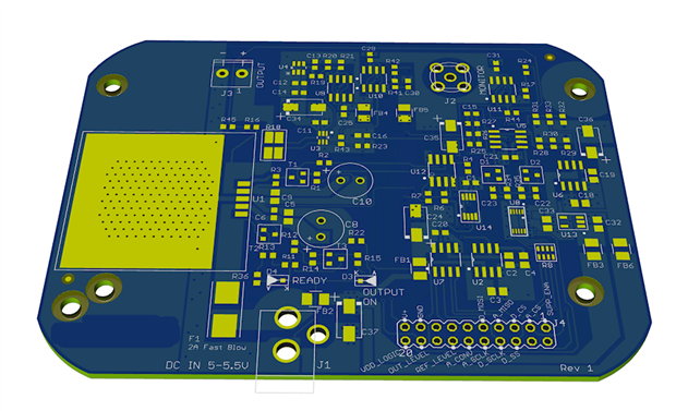
This part 2 discusses some of the PCB layout (more details once the board has arrived and been tested!). Note: The board was not designed for production, and PCB layout engineers will take many different decisions compared to the design here. However the general layout is described here for those interested in following the project (layout and schematics will be published so others can build it too).

image


PCB Layout Decisions

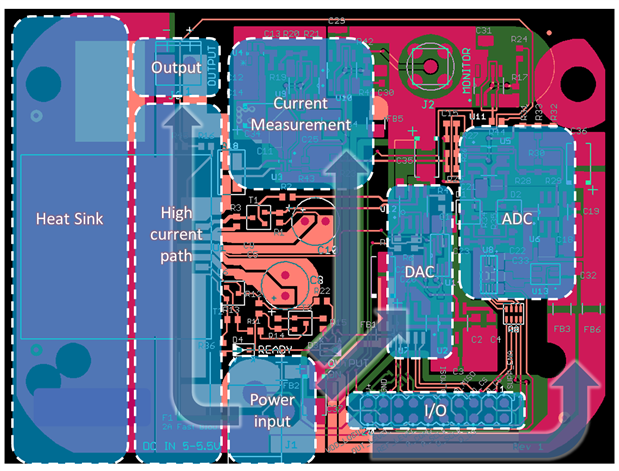
The approximate functional areas are shown below, and the paths (and returns for power planes). The highest frequency signals will be around the ADC, and it was kept furthest away from the remainder circuitry.


The path for the high current portion of the design is on the left side. There are multiple power and ground planes, all returning to a common point, which is not always feasible (and not always necessary) but was possible in this case. The aim is to always follow the high current signals and avoid supplying or referencing off them from different points, because whenever high current is flowing, there will be a voltage drop across different points on the same path (since V=IR and all traces have a certain resistance) which may affect any circuitry sensitive to voltage.

image


Often there are many other objectives too, such as avoiding capacitive or inductive coupling or RF pickup or thermal effects from having a significant influence, depending on the types of circuits on the board. Some things can be solved at the component level (e.g. matched transistors, or shielded inductors) whereas others need board-level or entire assembly-level support (e.g. through distance between components or traces or planes, and shielding of circuitry).


Bypass capacitors are essential to provide low impedance to AC signals. A good general rule is to always follow the datasheet, otherwise if not specified, use a 100nF ceramic capacitor for circuits operating at frequencies up to a few tens of MHz. Any higher, and a 1nF capacitor should be used. In the several hundred MHz range, a 100pF capacitor should be used. The reason for these values is that capacitor inductive component becomes significant and limits the range that capacitors can be used at. The values above are rules of thumb. For higher frequencies, the datasheets should be consulted.


Zero-ohm resistors in line with signals are a great way of isolating circuitry, especially for a first PCB where you may want to isolate bits of circuitry.


To start the layout, the first step was to approximately sketch the sub-circuits, so that they could be moved around to plan it (like planning the layout of a room):

image

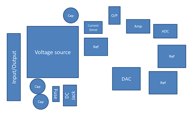
The final layout (shown earlier) looks different from the one above, but some parts of the circuit can be seen to be in similar positions to this initial thought.


Copper areas were created using ‘polygon’ elements in EAGLE. It is worth spending time learning how to use them because they are essential for power planes.


Via holes were kept large to allow low-cost PCB manufacturers to be used, which meant that in a few places they could not be avoided in the pad area, and were placed as far out from the center of pads as possible. This is not usually an issue for hand-soldered boards.


Regarding trace width, if current is expected to be high or resistance will have an effect on a particular signal then thick or short traces are needed; for digital signals often thinner traces are better to reduce capacitive coupling (I avoid the absolute minimum that the manufacturer supports, and choose a width perhaps 1/3 higher), and route them away from analog portions.


Another consideration is how the board will be cased; for flexibility there are holes with different spacings so that the board should hopefully fit several different enclosures. I chose 50, 85 and 90mm spacings, and also cut off all corners. Lots of space is needed around screw holes, so it is good to dedicate this space early before spending time routing signals.


For text on the PCB, a good size is 1.27mm height; this is very readable from a distance yet small enough to fit in most places. If this size is not possible then I reduce to 0.9mm height which is still readable but small. Smaller that this is possible too, but I avoid going further than that.


Space may be needed for labels, and 30mm or more is not unusual. Logos were created by using EAGLE’s import-bmp program (also known as a user language program or ULP in EAGLE terminology).


EAGLE’s ‘Smash’ option is used to separate labels from the component packages, so that text can be moved around. I chose to only have the component references on the silkscreen, and not the component values.


Since there may be multiple copies of this project floating around the lab, it was decided to electronically label each one, either with an electronic serial number or programmable memory. This makes it possible to retain history for each board such as calibration data or board revision numbering so that the same software can be used with multiple boards. I used serial EEPROM.

image

Post 3 will follow hopefully early in the new year!

Attachments:
imagemain.pdf
  • Sign in to reply

Top Comments

  • michaelkellett
    michaelkellett over 10 years ago in reply to shabaz +2
    For what it's worth here's my take on an all analogue version. All parts from Linear Technology just because it's easier to model them in LT Spice than any other way. Key things are that R5=R4 and the…
  • mcb1
    mcb1 over 10 years ago +1
    Sounds like a very useful item. The electronic tag is a great idea, and as you point out can be used for calibration reference checks. Thanks Mark
  • jw0752
    jw0752 over 10 years ago +1
    Hi Shabaz, You have time to do all this beautiful work and still have time left over to help a friend get his little oscillator going. I will continue to follow your project as it is very interesting.…
Parents
  • michaelkellett
    michaelkellett over 10 years ago

    Are you attempting to model the battery impedance as well as discharge ?

    (I couldn't work out if the series resistor is a fixed part or a dynamically simulated part from your first blog).

    Will you post a schematic (or have I missed it) ?


    MK

    • Cancel
    • Vote Up +1 Vote Down
    • Sign in to reply
    • More
    • Cancel
Comment
  • michaelkellett
    michaelkellett over 10 years ago

    Are you attempting to model the battery impedance as well as discharge ?

    (I couldn't work out if the series resistor is a fixed part or a dynamically simulated part from your first blog).

    Will you post a schematic (or have I missed it) ?


    MK

    • Cancel
    • Vote Up +1 Vote Down
    • Sign in to reply
    • More
    • Cancel
Children
  • shabaz
    shabaz over 10 years ago in reply to michaelkellett

    Hi Michael!


    The resistor will be dynamically simulated, which will be interesting to see if it works! I've tried to constrain the problem since the expected loads will be low (wireless nodes intended for battery power, so a few hundred mA and 4.2V ballpark), and am hoping that if I can respond within about 100usec (i.e. within the time constant of a small supply capacitor) then it might be able to perform the simulation. Current is measured at about 10ksps and the voltage update is at this rate too. To save costs voltage is not measured on-board, but instead the voltage level is routed (scaled down) to the I/O connectors since most microcontroller boards have a built-in ADC. So basically the board concentrates on (moderately fast) current measurement and voltage control response; the voltage measurement (and of course any algorithms/lookup tables) are delegated to the connected microcontroller board.

    The selected parts will run at 10x the rates mentioned, but I'm hoping I can get a reasonable simulation at a lower speed to give more time to the microcontroller for doing its tasks.

    Does this sound a reasonable method?

    • Cancel
    • Vote Up 0 Vote Down
    • Sign in to reply
    • More
    • Cancel
  • shabaz
    shabaz over 10 years ago in reply to michaelkellett

    (Schematic now attached to the main post - I was going to do a walk-through of it in the next post, but for those interested in the project it might be helpful to see it now to get a rough idea).

    Some things may be tweaked during test, in which case I'll update with a revised schematic.

    • Cancel
    • Vote Up 0 Vote Down
    • Sign in to reply
    • More
    • Cancel
  • michaelkellett
    michaelkellett over 10 years ago in reply to shabaz

    Sounds perfectly reasonable in principle (I haven't done any sums re. sampling rates and ADC resolution) - it'll tend to struggle with very low or very high impedances because the convertor errors will be a problem. For example, if you try to simulate  a very low source impedance you will be measuring only a small voltage difference, the problem will be to prevent the control algorithm from injecting quantisation noise - so you may need better than a 12 bit on chip type ADC. But at 10kHz sampling rate you have time for lots of processing with even a cheap uP (I'd use an STM32F4xx for the 168MHz clock) so it is possible to have very smart control.

    If I were doing it I would simulate it with MATLAB (and SIMULINK) first.


    MK

    • Cancel
    • Vote Up 0 Vote Down
    • Sign in to reply
    • More
    • Cancel
  • shabaz
    shabaz over 10 years ago in reply to michaelkellett

    I regret I didn't do a whole system simulation in MATLAB, it would have indeed have benefited this project (I did simple calculations in MS Excel) : (

    • Cancel
    • Vote Up 0 Vote Down
    • Sign in to reply
    • More
    • Cancel
  • michaelkellett
    michaelkellett over 10 years ago in reply to michaelkellett

    I've had a look at your circuit - I'm not sure if you've actually ordered boards yet - in which case the following remarks are not going to be very useful.

    I think I would have wanted a way of getting  a zero reference on the current - so as to eliminate the zero drift that you'll see because of relative and absolute drifts in the reference voltage for U3 and the biasing of U5.

    I'm guessing that you have a full scale current of about 1A which will give 30mV across R18, 3V on R234 and a swing of 2.7V on the ADC inputs. 18 bits down on that is about 4uA which is only 0.12uV across R18 but the offset error from U3 will be typically 1 but possibly up to 60uV (TI aren't very clear about when it gets really bad). Any way the point is that your minimum measurable current is set by the voltage drop across R18 and potentially quite a lot of the ADC range won't be useable.

    The obvious response is to make R18 switchable but this isn't helpful because you then end up with a bunch of relays etc trying to keep up with a sudden increase in current demand.

    I think I would have made R18 at least 1R and put it on the other side of the voltage control device  - of course you couldn't use an LDO but you could have used a MOSFET.

    I would have tried to use just one precision voltage reference - the only one that has to be really good is the one for the ADC so I'd have kept that one, done the offset for U3 by potting don the ADC reference and just used power supply (or U6)  for the DAC because the accurate output voltage is controlled by the ADC in the end.


    I think what you have will work OK, but that you could squeeze a lot more out of the 18bit ADC.


    MK

    • Cancel
    • Vote Up 0 Vote Down
    • Sign in to reply
    • More
    • Cancel
element14 Community

element14 is the first online community specifically for engineers. Connect with your peers and get expert answers to your questions.

  • Members
  • Learn
  • Technologies
  • Challenges & Projects
  • Products
  • Store
  • About Us
  • Feedback & Support
  • FAQs
  • Terms of Use
  • Privacy Policy
  • Legal and Copyright Notices
  • Sitemap
  • Cookies

An Avnet Company © 2025 Premier Farnell Limited. All Rights Reserved.

Premier Farnell Ltd, registered in England and Wales (no 00876412), registered office: Farnell House, Forge Lane, Leeds LS12 2NE.

ICP 备案号 10220084.

Follow element14

  • X
  • Facebook
  • linkedin
  • YouTube