On October 19, 2020, Arm announced the Arm Ethos
-U65 microNPU. A NPU is a neural processing unit and a microNPU is, as the name implies, a very small NPU, often targeted for area-constrained embedded and IoT devices. Big deal you may be thinking, but by the end of this blog, hopefully you will come around to agreeing that this one is a big deal.
Back in February 2020, NXP announced its lead partnership for the Ethos-U55 microNPU for Arm Cortex-M systems. The Ethos-U55 is designed for microcontrollers and works in concert with the Cortex-M processor and system SRAM and flash in a MCU to deliver both the combination of performance and efficiency that MCU customers demanded. But the Ethos-U55 wasn’t necessarily an obvious fit for sophisticated ML applications running locally at the edge on Cortex-A-based applications processors.
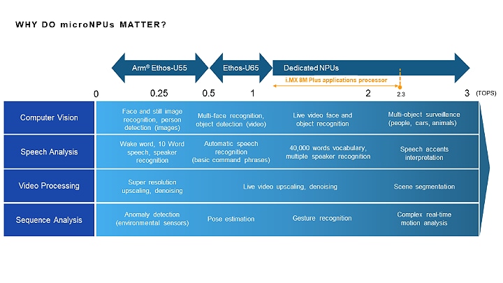
Through our technology partnership with Arm, our two teams began working very closely together on the Ethos-U55 architecture, and in the process, realized that an additional microNPU that maintains the power efficiency of the Ethos-U55, while extending its applicability to Arm Cortex-A based systems, could be a good fit for heterogeneous SoCs such as NXP’s i.MX family for the industrial and IoT Edge. Working together we were able to increase performance of the Ethos-U55, not just in doubling the maximum raw MAC (multiply and accumulate) performance up to 1.0 TOPS (512 parallel multiply-accumulate operations at 1GHz operating frequency), but also right-sizing system buses to feed data into and out of the microNPU. But that wasn’t enough. MCUs are typically a mixture of SRAM and flash-based in their memory usage, but Cortex-A-based applications processors generally have DRAM. DRAM offers much higher data rates and capacities, but comes at the cost of longer latency. The microNPU needed to be designed to accommodate this latency. This was all achieved and became the Ethos-U65.
Like the Ethos-U55, the Ethos-U65 microNPU works in concert with the Cortex-M core and on-chip SRAM already present in NXP’s i.MX family. Under the hood, it inherited all the MCU-class power efficiency of the Ethos-U55. This Cortex-M and Ethos-U combination results in improved area and power efficiency compared to conventional NPUs, enabling the development of cost-effective, yet high performance edge ML products.
Also like the Ethos-U55, the Ethos-U65 software model relies on offline model compilation and optimization for the chosen underlying hardware. This is something that PCs or cell phones do not generally do, as by contrast their focus is on having a precompiled binary capable of running on a large variety of target hardware. But in embedded markets in the industrial and IoT Edge, the underlying hardware is generally known and needs to be utilized as efficiently as possible. This offline compilation optimizes for the specific Ethos-U65 configuration as well as the amount of on-chip SRAM that the user decides to allocate to the Ethos-U65. The result maximizes key data being stored in on-chip SRAM, with less frequent data usage spilling over to system DRAM.
The results are quite impressive. For example, according to Arm, the 512GOPS implementation of Ethos-U65 running at 1GHz is capable of object recognition in less than 3ms when running the popular MobileNet_v2 deep neural network. This is at least ten times faster inference performance compared to executing on quad-core Cortex-A53 running at 2GHz. There is still headroom in the ML-enabled market space above the Ethos-U65 for products such as NXP’s i.MX 8M Plus SoC (announced in January 2020) with its up to 2.3 TOPS NPU. But the Ethos-U65 fills a sweet spot in the Industrial and IoT Edge market for products and use cases that do not require the raw processing power of the i.MX 8M Plus, but demand even more stringent MCU-class efficiency.

To learn more about the Arm Ethos-U65 microNPU please see Arm’s blog.
Read the press release.

